Manufacturing process of transient voltage suppression diode chip
What is Al technical title?
Al technical title is built by PatSnap Al team. It summarizes the technical point description of the patent document.
A technology of transient voltage suppression and manufacturing process, applied in semiconductor/solid-state device manufacturing, circuits, electrical components, etc., can solve problems such as increased reverse leakage current, reduce reverse leakage current, eliminate stress and defects, The effect of voltage distribution concentration
Active Publication Date: 2014-02-26
南通康芯半导体科技有限公司
View PDF2 Cites 26 Cited by
Summary
Abstract
Description
Claims
Application Information
AI Technical Summary
This helps you quickly interpret patents by identifying the three key elements:
Problems solved by technology
Method used
Benefits of technology
Problems solved by technology
[0005] like figure 1 As shown, the first layer of the PN junction interface of the P (boron) region 33 is the glass passivation layer 44. There is still a relatively high concentration of interface states at the interface between silicon and glass, and there are microbubbles in the glass on the interface, which makes the device work. Increased reverse leakage current
Method used
Image
Click on the blue label to locate the original text in one second.
Reading with bidirectional positioning of images and text.
Examples
Embodiment Construction
[0026] The present invention will be described in further detail below in conjunction with the accompanying drawings and specific embodiments.
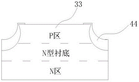
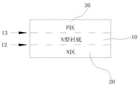
[0027] like Figure 2 to Figure 5 A manufacturing process of a transient voltage suppression diode chip according to an embodiment of the present invention is schematically shown.
[0028] The manufacturing process of the transient voltage suppression diode chip of the present invention includes two production processes: a diffusion process and a GPP process.
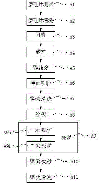
[0029] like figure 2 and image 3 As shown, the steps of the diffusion process include:
[0030] A1: Original silicon wafer test, test the resistivity and thickness of the original silicon wafer to ensure the accuracy of feeding. Select N-type silicon material double lapped wafers with a resistivity of 0.04-0.05Ω.cm and a thickness of 295-305μm.
[0031] A2: Clean the original silicon wafer to remove impurities on the surface of the original silicon wafer, so as not to af...
PUM
Abstract
The invention discloses a manufacturing process of a transient voltage suppression diode chip. The manufacturing process of the transient voltage suppression diode chip includes two production processes: a diffusion process and a GPP process. The steps of the diffusion process include original silicon wafer testing, original silicon wafer washing, phosphorus attachment, phosphorus diffusion, phosphorus wafer separation, single side sand blasting, single blasting washing, boron coating, boron diffusion, boron wafer separation, boron side sand blasting, and boron blasting washing, wherein the step of boron diffusion comprises primary boron diffusion and secondary boron diffusion; and the steps of the GPP process sequentially include oxidation, primary photoetching, groove etching, photoresist sintering, groove washing, SIPOS passive film formation, glassivation, secondary photoetching, surface etching, and nickel-gold plating. The manufacturing process of the transient voltage suppression diode chip in the invention reduces defects of the chip, enables voltage distribution to be relatively concentrated, and reduces reverse leakage current at the same time.
Description
technical field [0001] The invention relates to the manufacturing field of a semiconductor device, in particular to a manufacturing process of a transient voltage suppression diode chip. Background technique [0002] Today's transient voltage suppression diode chip manufacturing process is divided into diffusion process and GPP process. [0003] The diffusion process steps are: original silicon wafer test → original silicon wafer cleaning → phosphorus addition → phosphorus diffusion → phosphorus crystal separation → single-side sand blasting → single blowing cleaning → boron coating → boron diffusion → boron crystal separation → boron blowing → boron blowing cleaning . Among them, the boron-coated silicon wafer is only subjected to boron diffusion once, and the process is as follows: push the silicon wafer into a diffusion furnace at 500°C, control the temperature of the diffusion furnace to rise to 1262°C at a rate of 5°C / min, and keep the temperature at 1262°C for 10 hour...
Claims
Application Information
Patent Timeline
Application Date:The date an application was filed.
Publication Date:The date a patent or application was officially published.
First Publication Date:The earliest publication date of a patent with the same application number.
Issue Date:Publication date of the patent grant document.
PCT Entry Date:The Entry date of PCT National Phase.
Estimated Expiry Date:The statutory expiry date of a patent right according to the Patent Law, and it is the longest term of protection that the patent right can achieve without the termination of the patent right due to other reasons(Term extension factor has been taken into account ).
Invalid Date:Actual expiry date is based on effective date or publication date of legal transaction data of invalid patent.