Crystalline silica solar cell chip diffusion method

A technology for solar cells and crystalline silicon wafers, applied in the directions of crystal growth, diffusion/doping, chemical instruments and methods, etc., can solve the problem of low-efficiency crystalline silicon solar cells, poor uniformity of surface sheet resistance, poor short-wave response of cells, etc. problem, to achieve the effect of low cost, high conversion efficiency and uniform diffusion

Active Publication Date: 2014-03-05
SUZHOU AIKANG PHOTOELECTRIC TECH CO LTD
View PDF8 Cites 34 Cited by
  • Summary
  • Abstract
  • Description
  • Claims
  • Application Information

AI Technical Summary

Problems solved by technology

[0002] Diffusion is an important process in the production process of crystalline silicon solar cells. The traditional diffusion process uniformly dopes the surface of crystalline silicon solar cells. High, but the high impurity concentration on the surface leads to band shrinkage in the diffusion region, lattice distortion, increased defects, obvious "dead layer", poor short-wave response of the battery; in order to obtain high-efficiency crystalline silicon solar cells with good short-wave response, the crystalline silicon wafer Diffusion develops in the direction of high square resistance
The current diffusion method for crystalline silicon solar cells is as follows: place the crystalline silicon wafer in a horizontal diffusion furnace cavity, and pass in a mixed gas, which is composed of nitrogen and phosphorus oxychloride in proportion, and is in a state of normal pressure. Diffusion of crystalline silicon wafers, the uniformity of the surface sheet resistance in the crystalline silicon wafers obtained after diffusion processing is poor, and when high surface sheet resistance is produced, it is easy to cause low-efficiency crystalline silicon solar cells in the subsequent production process

Method used


Image

  • Crystalline silica solar cell chip diffusion method

Examples


Embodiment Construction

[0019] The technical solutions of the present invention will be further described in detail below in conjunction with the accompanying drawings and preferred embodiments.

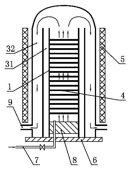
[0020] Such as figure 1 Shown is a schematic structural view of a vertical diffusion furnace used in a crystalline silicon solar cell diffusion method according to the present invention, consisting of an inner furnace chamber 31, an outer furnace chamber 32, and an air inlet 7 at the bottom of the inner furnace chamber 31 , an air extraction port 9 located at the bottom of the outer furnace chamber 32, a furnace door 6, an insulating layer 8, a heater 5 arranged on the outer wall of the furnace body, and a quartz boat 1 for loading crystalline silicon wafers 4. The inner and outer furnace chambers The tops of 31 and 32 communicate with each other. Select a P-type 156×156mm polycrystalline silicon wafer, use hydrofluoric acid or nitric acid to clean the surface oil and texture the crystalline silicon wafer ...


PUM


Abstract

The invention discloses a crystalline silica solar cell chip diffusion method. Hydrofluoric acid or nitric acid is used for cleaning oil stain on the surface of a silicon chip and etching the surface of the silicon chip, the cleaned and etched silicon chip is placed in a vertical diffusion furnace to be diffused, and the diffusion technology includes following steps of (1) putting into the furnace: putting a quartz boat containing crystalline silica chips into the furnace at a uniform speed; (2) carrying out vacuum-pumping, wherein the pressure in a furnace chamber is 300 +/-50 mTorr after the step of vacuum-pumping; (3) carrying out vacuum leak detection on the furnace chamber; (4) carrying out oxidation in low pressure; (5) carrying out first phosphor source diffusion in low pressure; (6) heating; (7) carrying out second phosphor source diffusion in low pressure; (8) carrying out phosphor impurity propulsion in low pressure; (9) cooling; and (10) taking out form the furnace. By adopting the above crystalline silica solar cell chip diffusion method, the molecule free path of impurity is raised and the uniformity of diffusion of the crystalline silica chip is improved during diffusion, and the conversion efficiency of the crystalline silica solar cell chip is high; and the diffusion method is easy to operate, large in output and low in cost.

Description

technical field [0001] The invention relates to the field of production of solar cells, in particular to a method for diffusing crystalline silicon solar cells. Background technique [0002] Diffusion is an important process in the production process of crystalline silicon solar cells. The traditional diffusion process uniformly dopes the surface of crystalline silicon solar cells. High, but the high impurity concentration on the surface leads to band shrinkage in the diffusion region, lattice distortion, increased defects, obvious "dead layer", and poor short-wave response of the battery; in order to obtain high-efficiency crystalline silicon solar cells with good short-wave response, the crystalline silicon Diffusion develops in the direction of high square resistance. The current diffusion method for crystalline silicon solar cells is as follows: place the crystalline silicon wafer in a horizontal diffusion furnace cavity, and pass in a mixed gas, which is composed of ni...

Claims


Application Information

Patent Timeline
Patent Type & Authority Applications(China)
IPC IPC(8): H01L31/18C30B31/06
CPCC30B31/165H01L31/1804H01L31/186Y02E10/547Y02P70/50
Inventor 吴胜勇
Owner SUZHOU AIKANG PHOTOELECTRIC TECH CO LTD
Why Eureka
Try Eureka