Nano-silver conductive ink and conductive film prepared by employing same

A technology of conductive ink and conductive film, applied to the conductive layer on the insulating carrier, cable/conductor manufacturing, ink, etc., can solve the problems of increasing the difficulty and complexity of the manufacturing process, the detachment of the nanowire substrate, and the impact of product yield. Effective control of flatness, avoiding protection problems, and simplifying the production process

Active Publication Date: 2014-03-12
珠海纳金科技有限公司
View PDF6 Cites 79 Cited by
  • Summary
  • Abstract
  • Description
  • Claims
  • Application Information

AI Technical Summary

Problems solved by technology

[0003] At present, there have been many patent applications for transparent conductive films based on silver nanowires, but the usual processing technology is relatively complicated, and it takes several steps of transfer printing or repeated coating processes to finally achieve the required results.
Chinese patent applications 200910112924.X and 200910112925.4 disclose a method for preparing a transparent conductive film based on silver nanowires. The core idea is to increase the adhesion of silver nanowires on the substrate by adding an adhesion layer between the substrate and the nanowire conductive layer. Efforts have been made to basically solve the problem that the nanowires are easy to detach from the substrate, but the method used is relatively complicated, and the pre-prepared nanowire network needs to be transferred to the adhesion layer by transfer printing, which not only increases the difficulty of the process...

Method used


Image

  • Nano-silver conductive ink and conductive film prepared by employing same
  • Nano-silver conductive ink and conductive film prepared by employing same
  • Nano-silver conductive ink and conductive film prepared by employing same

Examples


Embodiment 1

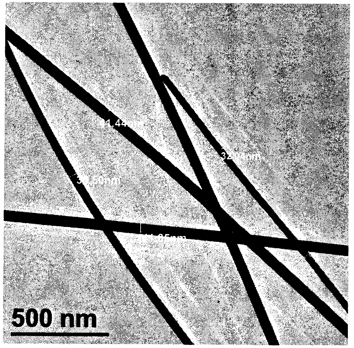
[0045] First, take 2.0g of SK polyester resin, dissolve 1g of cellulose acetate butyrate in 310g of ethyl lactate, add 0.01g of non-ionic fluorocarbon surfactant after complete dissolution, stir and mix until completely dissolved, then add 0.2g of leveling agent in turn (TEGO Glid 130), 0.1g rheology modifier (BYK-431), and then add 660g of ethanol solution containing 5g of nano-silver wires, wherein the average diameter of nano-silver wires is 40nm, the length is 30-50μm, and the aspect ratio exceeds 600, add 2g of anti-sedimentation agent (dibutyl phthalate), grind in a ball mill for 4 hours, and then mix it evenly with a disperser for 10 minutes to obtain a nano-silver wire conductive ink. The concentration of the nano-silver wire is 5mg / ml .

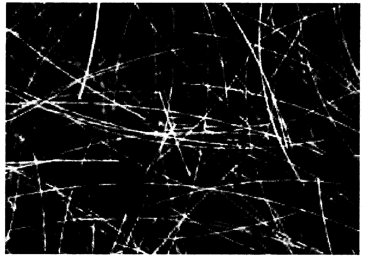
[0046] Polyethylene terephthalate (PET) is used as a transparent flexible substrate, its own light transmittance is 92%, and its thickness is 188 μm. The nano-silver wire conductive ink prepared above was evenly coated on the surfac...

Embodiment 2

[0052] Take 200g hydroxypropyl methylcellulose (HPMC) solution (3%, water and ethanol is 72:25), 0.75g Bayer curing agent W-8035 (40%), 10g Digao dispersant disperse760W (1%), 10g TEGO Wet 500 (1%), add mixed solvent (72:25 of water and ethanol) to 500g and stir evenly, add 0.5g rheology modifier BYK-425, 0.2g TEGO Wet270, 0.2g TEGO Glid110, Then take 262g of silver nanowire ethanol solution (average diameter 40nm, 5mg / ml), grind it in a ball mill for 4 hours, disperse it in a disperser for 10 minutes and stir evenly, and finally add ethanol to 1000g.

[0053] Using polycarbonate (PC) as a transparent flexible substrate, its own light transmittance is 92%, and its thickness is 125 μm. Apply the nano-silver wire conductive ink prepared above evenly on the surface of the PC substrate to form a uniform 15-30μm liquid film, dry it in a tunnel oven at 60°C, and heat it while pressing In the treatment, the heating temperature is 140° C., the heating pressure is 5 MPa, the pressure ...

Embodiment 3

[0055] Preparation of nano-silver wire conductive ink:

[0056] Get 20g mixed resin solution (solid content 2.73%, hydroxypropyl methylcellulose and aqueous polyester resin 830 solid content ratio 1: 1, solvent is water and ethanol 72: 25), the Bayer curing agent 2805 of 0.75g (40 %), 10g Digao dispersant TEGO Disperse760W (1%), 3g TTMAP, 10g Digao leveling agent TEGO Glid 100 (1%), add mixed solvent (water and ethanol is 72: 25) to 500g and stir evenly, then take 262g silver nanowire ethanol solution (average diameter 40nm, 5mg / ml) was stirred evenly, and ethanol was added to 1000g.

[0057] Using PET as a transparent flexible substrate, its own light transmittance is 92%, and its thickness is 100 μm. Apply the nano-silver wire conductive ink prepared above evenly on the surface of the PET substrate to form a uniform liquid film, and dry it in a tunnel oven at 120°C to obtain an overall conductive flexible transparent conductive ink without electrode patterns. membrane. Fi...


PUM

PropertyMeasurementUnit
The average diameteraaaaaaaaaa
Lengthaaaaaaaaaa
Thicknessaaaaaaaaaa

Abstract

The invention discloses nano-silver conductive ink and a conductive film prepared by employing the same. The technical scheme is characterized in that the nano-silver conductive ink is prepared, satisfies the requirements on light transmittance, film electrical resistance and adhesive force, is applicable to production of the conductive film; and the prepared conductive film is effectively controlled in flatness and easy to etch, is capable of effectively satisfying the requirements on patterning of touch-control screens and display panels, and has extremely good utility value.

Description

technical field [0001] The invention relates to the field of nanometer materials, in particular to a nano silver conductive ink and a conductive film prepared by using the ink. Background technique [0002] As a functional film with high light transmittance and low sheet resistance, transparent conductive film is widely used in touch screens, display panels, electromagnetic shielding, LED displays, electroluminescent devices, and thin-film solar cells. Based on the shortcomings of traditional ITO transparent conductive films such as resource shortage, high price, and prone to defects, those skilled in the art are currently devoting themselves to developing new alternative materials for transparent conductive films. Among them, metal nanomaterials, especially nanosilver materials, have become the most promising alternative materials for commercial use. [0003] At present, there have been many patent applications for transparent conductive films based on silver nanowires, bu...

Claims


Application Information

Patent Timeline
IPC IPC(8): C09D11/52H01B5/14H01B13/00
Inventor 谷小虎丁轶黄友科王正元
Owner 珠海纳金科技有限公司
Why Eureka
Try Eureka