Method of preparing groove semiconductor power device
A technology for power devices and semiconductors, which is applied in the field of preparation of trench semiconductor power discrete devices, can solve the problems of poor advantage index of semiconductor devices, poor terminal structure, and difficult to generate.
- Summary
- Abstract
- Description
- Claims
- Application Information
AI Technical Summary
Problems solved by technology
Method used
Image
Examples
Embodiment 1
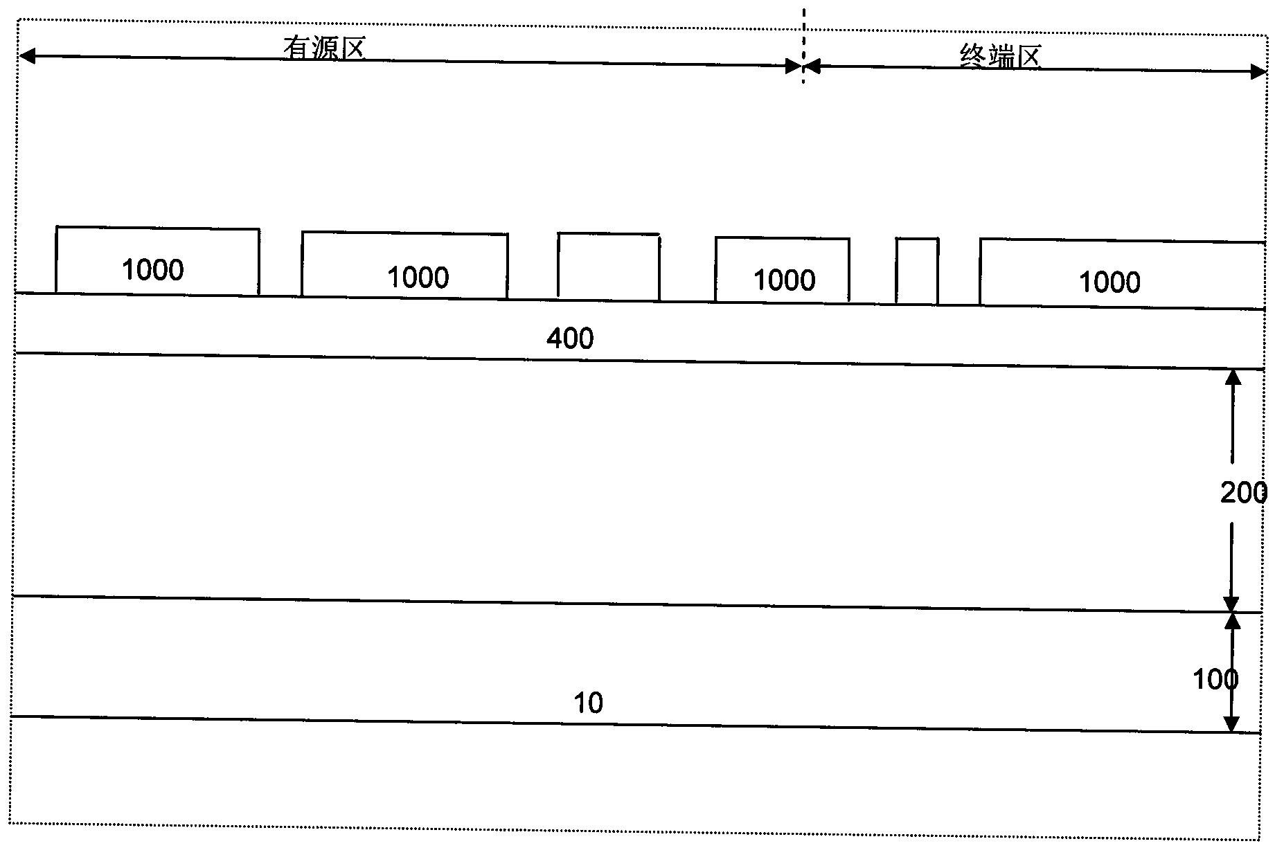
[0103] Such as figure 1 As shown, the p-type epitaxial layer 200 is first placed on the top of the n-type substrate 10, and then an oxide layer 400 (with a thickness of 0.3um to 1.5um oxide hard mask) is formed on the epitaxial layer by deposition or thermal growth. , depositing a layer of photoresist coating 1000 on the oxide layer, and then patterning through a trench mask to expose some parts of the oxide layer.
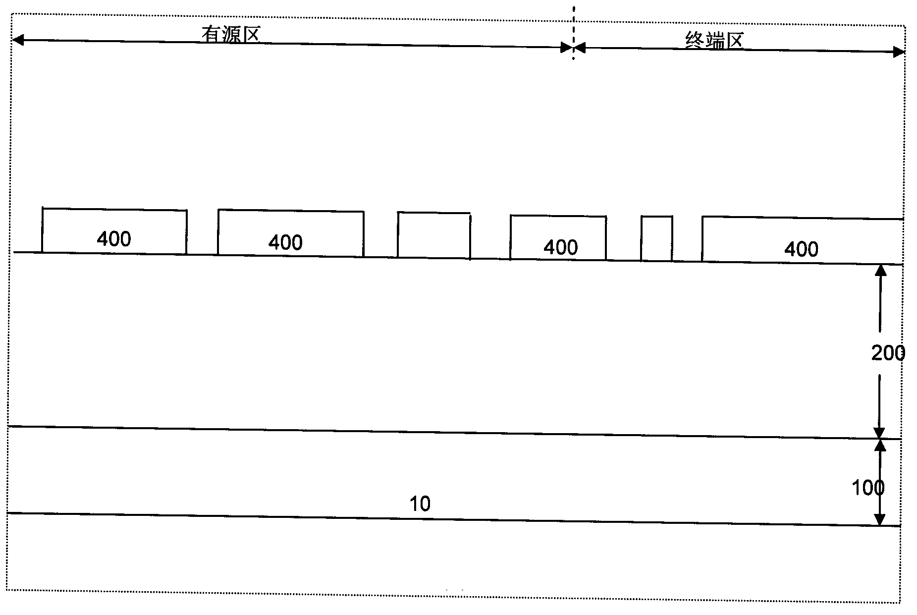
[0104] Such as figure 2 As shown, after dry etching the oxide layer exposed by patterning the trench mask, the epitaxial layer is exposed, and then the photolithographic coating is removed.
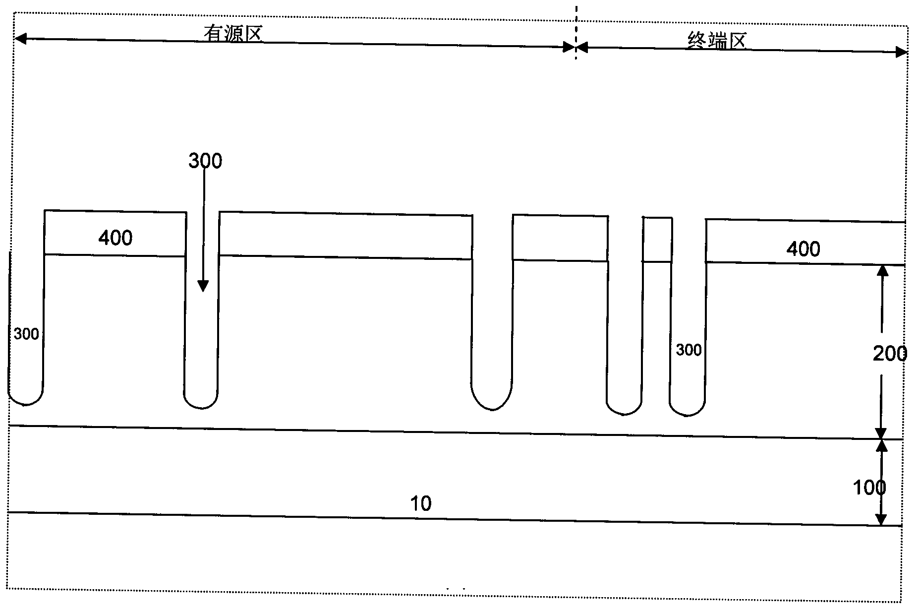
[0105] Such as image 3 As shown, trenches 300 (0.6um to 5.0um in depth and 0.12um to 1.5um in width) are formed by etching.
[0106] Such as Figure 4 As shown, after the trench is formed, the trench is sacrificially oxidized (the time is 10 minutes to 100 minutes, the temperature is 1000 ° C to 1200 ° C), in order to eliminate the silicon layer damaged by the plasma d...
Embodiment 2
[0123] It is an embodiment of the present invention.
[0124] Step and embodiment 1 are by Figure 1 to Figure 9 In the same way, a PSG oxide layer is formed on the surface of the silicon wafer and the top sidewall of the trench by deposition, with a thickness of 0.05um to 0.8um, and there is no need to form a non-doped oxide layer 501 on the surface of the silicon wafer and the top of the trench; Then planar etching or chemical mechanical polishing is performed on the oxide layer on the surface of the epitaxial layer to remove the PSG oxide layer on the surface of the epitaxial layer, and then a non-doped oxide layer is formed on the surface of the epitaxial layer by thermal growth or deposition. Layer, the thickness is 0.1um to 0.6um, remaining steps and embodiment 1 are by Figure 12 to Figure 19 same.
Embodiment 3
[0126] It is an embodiment of the present invention.
[0127] Step and embodiment 1 are by Figure 1 to Figure 12 In the same way, the N-type source region 203 is formed by using the source region mask step, and then the interlayer dielectric 503 is deposited on the surface of the epitaxial layer, and then the interlayer dielectric is eroded by using the contact hole mask to form an opening in the interlayer dielectric, Remaining steps and embodiment 1 are by Figure 16 to Figure 19 same.
PUM
 Abstract
Description
Claims
Application Information


