Intermediate infrared double-frequency-band metamaterial absorber based on double-L structure

An absorber and dual-band technology, applied in the field of metamaterials, can solve problems such as application limitations, and achieve the effects of simple structure, perfect absorption effect, and wide application prospects

Active Publication Date: 2014-03-26
HARBIN INST OF TECH
View PDF2 Cites 14 Cited by
  • Summary
  • Abstract
  • Description
  • Claims
  • Application Information

AI Technical Summary

Problems solved by technology

However, these studies mainly focus on the microwave, terahertz and visible light bands, and there are few reports on absorbers working in the mid-infrared band. The mid-infrared band absorber can be used as the absorbing unit of the thermal detector / emitter, or as a coating material to To reduce the spurious emission of electromagnetic waves, almost all existing mid-infrared absorbers have only one absorption band, which limits the application of mid-infrared absorbers in spectral detection, phase imaging of prohibited drugs and explosive materials, so we urgently need A multi-band, strong absorption mid-infrared absorber

Method used


Image

  • Intermediate infrared double-frequency-band metamaterial absorber based on double-L structure
  • Intermediate infrared double-frequency-band metamaterial absorber based on double-L structure
  • Intermediate infrared double-frequency-band metamaterial absorber based on double-L structure

Examples


Embodiment 1

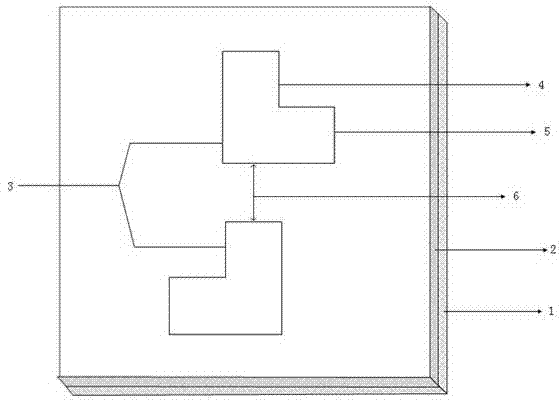
[0028] Such as figure 1 As shown, in this embodiment, a double-sided gold-coated silicon carbide dielectric substrate is selected. According to the wavelength corresponding to the absorption frequency band, the period of the absorber unit lattice is 2.6 , the medium thickness is selected as 0.27 , one side of the substrate is etched with a metal pattern 3 with a thickness of 0.1 , the other side is full metal film layer 1, the thickness is also 0.1 , the metal pattern 3 is made of gold, wherein the metal pattern 3 is composed of upper and lower L-shaped patterns, the two L-shaped patterns are arranged in the middle of the dielectric substrate 2, and each L-shaped pattern is composed of mutually perpendicular horizontal arms 5 It is connected with the vertical arm 4, and the arm length is 0.8 , with an arm width of 0.4 , the longitudinal displacement 6 between the vertical arms of the two L-shaped patterns is 0.1 , the lateral displacement between the vertical arm 4...

Embodiment 2

[0033] Such as figure 1 As shown, in this embodiment, a gallium arsenide dielectric substrate coated with gold on both sides is selected. According to the wavelength corresponding to the absorption frequency band, the period of the absorber unit lattice is 2.6 , the medium thickness is selected as 0.27 , one side of the substrate is etched with a metal pattern 3 with a thickness of 0.1 , the other side is full metal film layer 1, the thickness is also 0.1 , the metal pattern 3 is made of gold, wherein the metal pattern 3 is composed of upper and lower L-shaped patterns, the two L-shaped patterns are arranged in the middle of the dielectric substrate 2, and each L-shaped pattern is composed of mutually perpendicular horizontal arms 5 It is connected with the vertical arm 4, and the arm length is 0.8 , with an arm width of 0.4 , the longitudinal displacement 6 between the vertical arms of the two L-shaped patterns is 0.1 , the lateral displacement between the vertical...

Embodiment 3

[0035] Such as figure 1 As shown, in this embodiment, a double-sided gold-coated zinc selenide dielectric substrate is selected. According to the wavelength corresponding to the absorption frequency band, the period of the absorber unit lattice is 6.5 , the medium thickness is selected as 0.5 , one side of the substrate is etched with a metal pattern 3 with a thickness of 0.25 The other side is an all-metal film layer 1 with a thickness of 0.1 , the metal pattern 3 is made of gold, wherein the metal pattern 3 is composed of upper and lower L-shaped patterns, the two L-shaped patterns are arranged in the middle of the dielectric substrate 2, and each L-shaped pattern is composed of mutually perpendicular horizontal arms 5 Connected with the vertical arm 4, the arm length is 1.9 , with an arm width of 1 , the longitudinal displacement 6 between the vertical arms of the two L-shaped patterns is 0.4 , the lateral displacement between the vertical arm 4 and the cell bou...


PUM


Abstract

The invention provides an intermediate infrared double-frequency-band metamaterial absorber based on a double-L structure and belongs to the field of metamaterials. The absorber comprises a dielectric substrate with double sides covered with metal, wherein the back side of the dielectric substrate is provided with a metal film layer, and the front side of the dielectric substrate is provided with etched double-L metal array patterns consisting of an upper L-shaped pattern and a lower L-shaped pattern. Each L-shaped pattern is formed by connecting a horizontal arm and a vertical arm which are perpendicular to each other, a diagonal line formed by the tail ends of two arms of the upper L-shaped pattern is perpendicular to a diagonal line formed by the tail ends of two arms of the lower L-shaped pattern, and the vertical arms of the L-shaped patterns are arranged on the same line. By reasonably designing the geometric dimension and a lattice period of the L-shaped structure, electromagnetic waves incoming onto the surface of a metamaterial can be completely absorbed. The metamaterial absorber has the advantages of being simple in structure and large in incidence angle, performing absorption through an intermediate infrared band and being provided with two absorption peaks and has wide application prospect in the fields of electromagnetic energy absorption, spectrum detection and the like.

Description

technical field [0001] The invention belongs to the field of metamaterials and relates to a mid-infrared absorber, in particular to a mid-infrared dual-band metamaterial absorber based on a double-L structure. Background technique [0002] In the electromagnetic spectrum, the wavelength range is usually 0. 76~1000 This spectral range is called the infrared spectral region, which is further divided into near-infrared (0.76~2.5 ), mid-infrared (2.5~25 ) and far infrared (25~1000 ). Mid-infrared, also known as thermal infrared or emission infrared, can be used for infrared scanning imaging at night, and the fundamental frequency absorption bands of most organic and inorganic substances appear in the mid-infrared region, so it is of great importance to the research on the properties of materials in the mid-infrared band. significance. [0003] Electromagnetic metamaterial (Metamaterial) refers to an artificial composite structure or composite material with extraordinar...

Claims


Application Information

Patent Timeline
Patent Type & Authority Applications(China)
IPC IPC(8): G02B5/00
Inventor 姜永远赵丽白阳
Owner HARBIN INST OF TECH
Why Eureka
Try Eureka