Manufacturing method for GaN epitaxy or substrate

A fabrication method and epitaxy technology, applied in semiconductor/solid-state device manufacturing, electrical components, circuits, etc., can solve problems such as complex methods, and achieve the effects of simple process steps, strong operability, and alleviating GaN stress

Inactive Publication Date: 2014-03-26
SHANGHAI HUAHONG GRACE SEMICON MFG CORP
View PDF5 Cites 28 Cited by
  • Summary
  • Abstract
  • Description
  • Claims
  • Application Information

AI Technical Summary

Problems solved by technology

[0003] Chinese Invention Patent Application Publication (CN101514484, publication date: August 26, 2009) discloses that growing GaN epitaxy on a porous substrate can effectively prevent GaN stress and prevent GaN cracks, but the method is very complicated

Method used


Image

  • Manufacturing method for GaN epitaxy or substrate
  • Manufacturing method for GaN epitaxy or substrate
  • Manufacturing method for GaN epitaxy or substrate

Examples


Embodiment Construction

[0028] The present invention will be described in further detail below in conjunction with the accompanying drawings and embodiments.

[0029] Such as Figure 1-Figure 6 As shown, a GaN epitaxial manufacturing method of the present invention mainly includes the following steps:

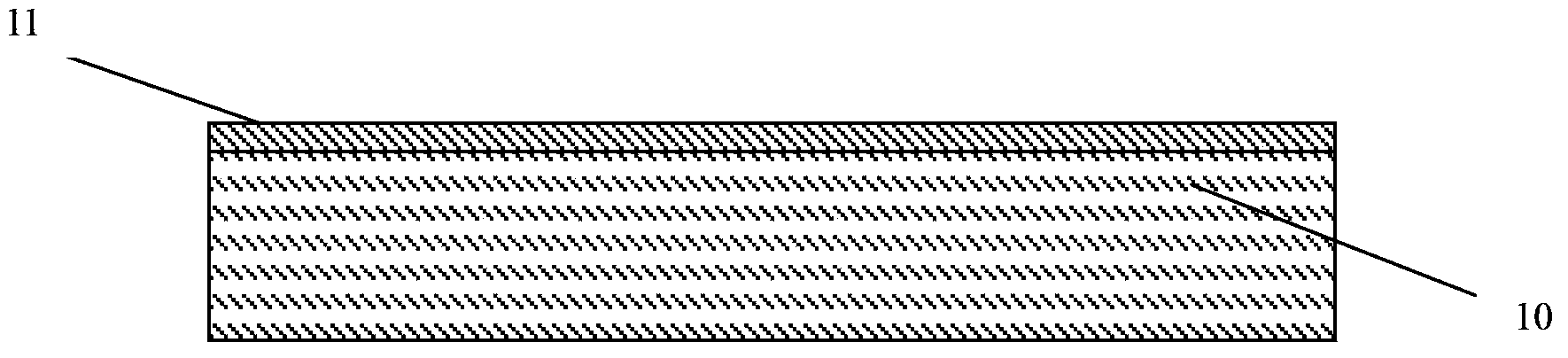
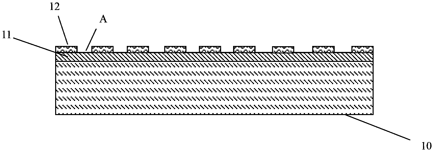
[0030] 1. Growth buffer layer 11 on silicon substrate 10, buffer layer 11 is AlN, Al 2 o 3 , GaN, AlAs, at least one of GaAs (see figure 1 ). The buffer layer 11 can be grown by MOCVD (Metal-organic Chemical Vapor Deposition, metal-organic compound chemical vapor deposition), ALD (atomic layer deposition), etc., and the thickness of the buffer layer 11 is 10-200 nm.

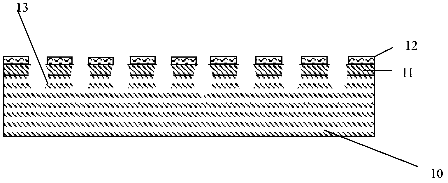
[0031] 2. The photoresist 12 is coated and exposed to form a defined pattern on the buffer layer 11: a plurality of circular areas A, the radius of each circular area A is 0.01-100 microns (in this embodiment, preferably 3 microns), The pitch is 0.1-100 microns (in this example, preferably 5 microns) (see figure 2 , Figure 7 )...


PUM

PropertyMeasurementUnit
thicknessaaaaaaaaaa
thicknessaaaaaaaaaa

Abstract

The invention discloses a manufacturing method for GaN epitaxy or substrate. The method provided by the invention comprises the following steps: 1), a buffer layer grows on a silicon substrate; 2), photoresisting coating and exposing are performed, and defined graphs are formed on the buffer layer; 3), a photoresist is used as a mask to etch the buffer layer and the silicon substrate, so as to enable a plurality of holes to be formed inside the silicon substrate; 4), the photoresist is removed; 5), thermal oxidation is performed on the inner surfaces of the holes inside the silicon substrate so as to enable the inner surfaces to be covered with monox; 6), the GaN epitaxy grows. The method can effectively relieve GaN stress, and prevents GaN cracking and GaN lattice defects.

Description

technical field [0001] The invention belongs to a semiconductor integrated circuit manufacturing process, in particular to a GaN epitaxy or substrate manufacturing method. Background technique [0002] GaN (gallium nitride) is a wide bandgap semiconductor material, which has excellent physical and chemical properties, such as large bandgap width, high breakdown electric field strength, high saturation electron drift velocity, high thermal conductivity and strong radiation resistance , large thermal conductivity and dielectric constant, stable chemical properties, etc., especially suitable for the production of semiconductor devices used in high-voltage, high-temperature, high-frequency, high-power, and strong-irradiation environments. Specifically, the band gap of GaN is larger than that of Si (silicon) material, and the intrinsic carrier concentration is lower than that of Si, which determines that the limit operating temperature of GaN-based devices is higher than that of ...

Claims


Application Information

Patent Timeline
Patent Type & Authority Applications(China)
IPC IPC(8): H01L33/32H01L33/00
CPCH01L21/02381H01L21/02513H01L21/0254H01L21/0262
Inventor 刘继全季伟许升高
Owner SHANGHAI HUAHONG GRACE SEMICON MFG CORP
Why Eureka
Try Eureka