Preparation method of flexible metal photonic crystal

A metal photonic crystal, flexible substrate technology, applied in nano-optics, optical waveguide light guide, nanotechnology and other directions, to achieve the effect of simple preparation method and efficient preparation process

Active Publication Date: 2014-04-02
BEIJING UNIV OF TECH
View PDF3 Cites 17 Cited by
  • Summary
  • Abstract
  • Description
  • Claims
  • Application Information

AI Technical Summary

Problems solved by technology

[0005] Metal photonic crystals with nanoscale periodici

Method used


Image

  • Preparation method of flexible metal photonic crystal
  • Preparation method of flexible metal photonic crystal
  • Preparation method of flexible metal photonic crystal

Examples


Embodiment 1

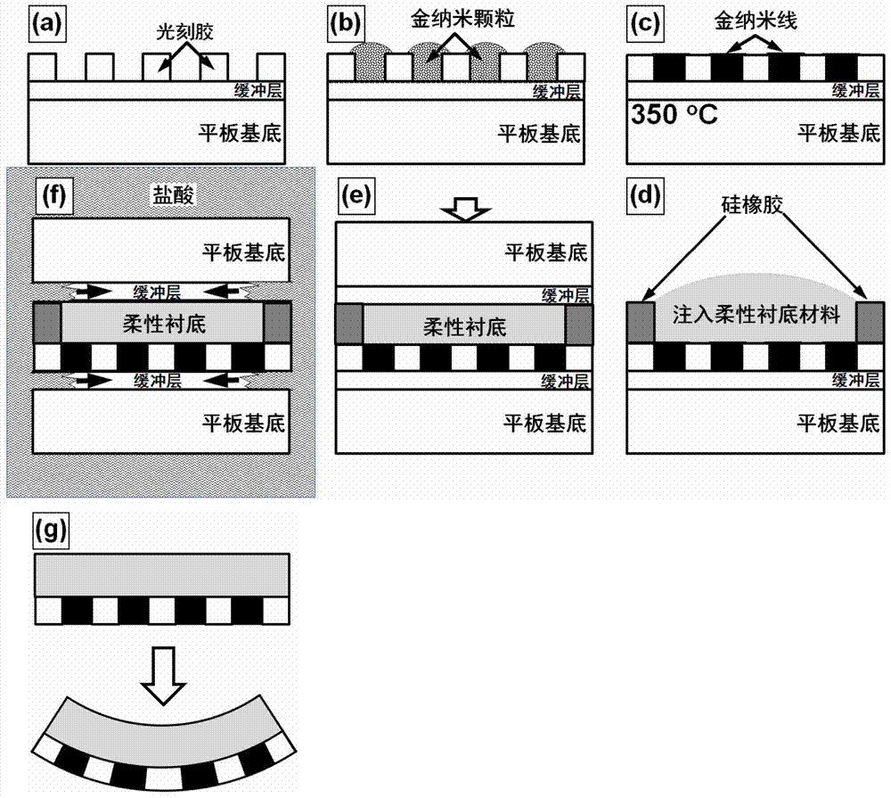
[0038] The present invention will be further described in conjunction with examples, but the present invention is not limited to the following examples. Example 1: Preparation of flexible metal photonic crystals.

[0039] (1) Spin-coat S1805 photoresist at 2000rpm on a glass substrate coated with a 200nm indium tin oxide (ITO) film.

[0040] (2) He-Cd laser with a wavelength of 325nm is used to carry out interference lithography in the S1805 photoresist film. The angle between the two laser beams participating in the interference lithography is controlled to be 48 degrees to ensure that the period of the photoresist grating is 400nm. The exposure time was controlled by an optical shutter for 20 s. Then develop in the developer for 6s. Then rinse with distilled water for 30 s. The cleaned sample was dried in an oven at 120° C. to obtain a photoresist grating structure.

[0041] (3) A colloidal solution of chemically synthesized gold nanoparticles in xylene with a concentra...

Embodiment 2

[0051] Example 2: Microstructure testing of flexible metal photonic crystals.

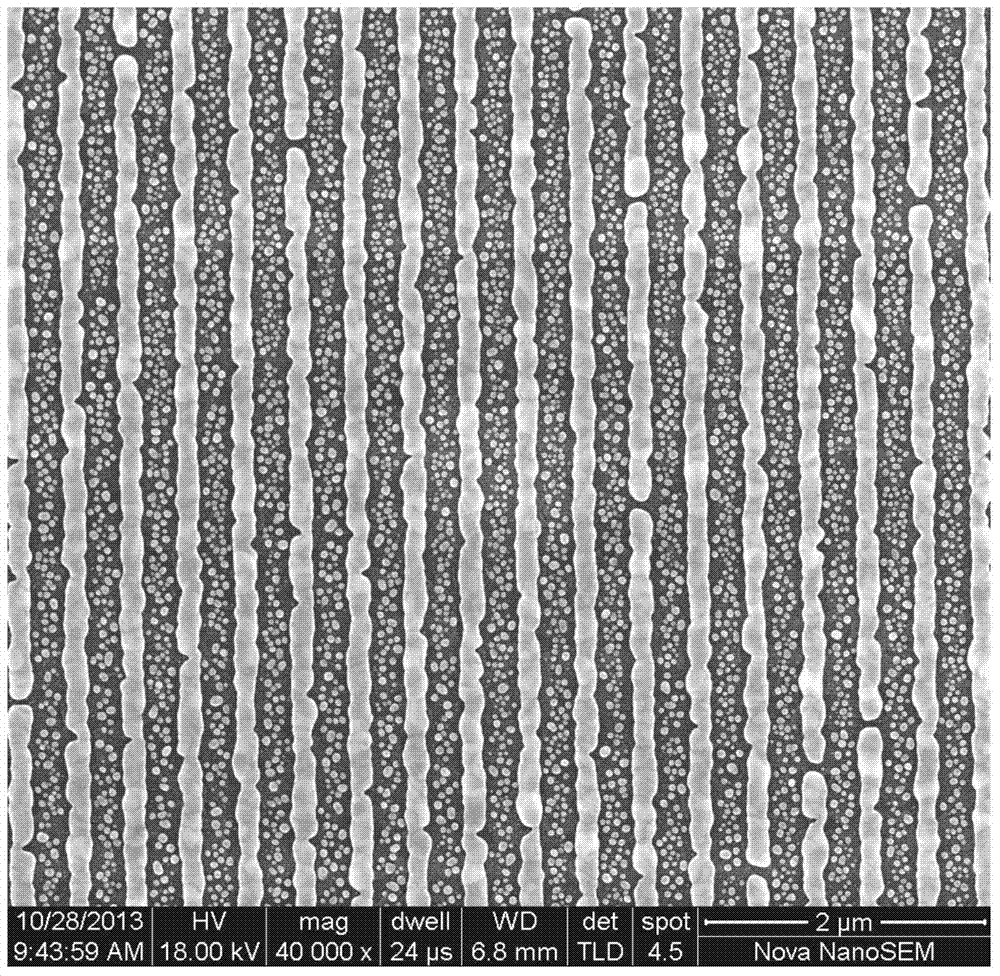
[0052] (1) adopt Nova NanoSEM type scanning electron microscope to measure the microstructure of the metal photonic crystal prepared in example 1 step 4, such as image 3 shown. Metal photonic crystals have a period of about 400nm and consist of periodically arranged gold nanowires. The average width of gold nanowires is about 165 nm. Some gold nanoparticles remain between the gold nanowires, and the diameters thereof are all less than 70nm.

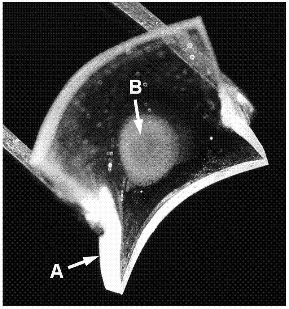
[0053] (2) The metal photonic crystal structure transferred to PDMS was measured by FEI Phenom desktop scanning electron microscope. Since the PDMS substrate is non-conductive, it is impossible to complete high-resolution electron microscopic measurement, that is, the testing instrument used in step (1) cannot be used. Test results such as Figure 4 shown. Since what is measured at this time is the bottom surface of the metal photonic crystal prepared o...

Embodiment 3

[0055] Example 3: Stretching realization of flexible metal photonic crystal and its stretching deformation sensor experiment.

[0056] (1) A self-built flexible photonic crystal tensile test platform is used, and the schematic diagram of the device is as follows Figure 6 As shown, the two ends of the PDMS substrate of the flexible metal photonic crystal are respectively fixed on two independent precision translation stages. Move the two translation stages separately to make them in the middle of the scale range, and add a certain initial stress to the PDMS substrate to ensure that the substrate is flattened. Except for the stretching direction, the substrate has no deformation and stress in other directions.

[0057] (2) A broadband white light source is focused to irradiate the metal photonic crystal on the PDMS substrate, and the transmitted light is accepted by the probe of the fiber optic spectrometer in order to measure the transmission spectrum.

[0058] (3) First col...


PUM

PropertyMeasurementUnit
Average widthaaaaaaaaaa
Diameteraaaaaaaaaa

Abstract

The invention discloses a preparation method of flexible metal photonic crystal and belongs to the technical field of nano photonic materials and devices. The method comprises the steps of preparing a photoresist nano grating structure on a buffer layer of a buffer layer substrate, dissolving and spin-coating gold nanoparticle colloid on the surface of grating and limiting the coating gold nanoparticle colloid in a groove of the grating, performing heating processing, so as to ensure that organic ligand on gold surface is sublimed and gold nanoparticle is fused, so as to form metal photonic crystal, coating flexible substrate liquid mixed with curing agent on the metal photonic crystal, covering another buffer layer substrate, heating the metal photonic crystal to perform cross-linking polymerization, putting the metal photonic crystal into a hydrochloric acid solution or a sulfuric acid solution, so as to sufficiently dissolve the buffer layer, and cleaning obtained samples through distilled water. The method has important direct application value for developing stress and deformation sensors and novel flexible optoelectronic devices.

Description

technical field [0001] The invention belongs to the technical field of nano-photonic materials and devices, and relates to a method for preparing a flexible metal photonic crystal. Background technique [0002] Metal photonic crystals are not only an important form of photonic crystals, but also a relatively independent form of nanophotonic structures due to their special photophysical properties such as plasmons. Metal photonic crystals have many irreplaceable application values ​​in optoelectronic technology, sensor technology and optical engineering, and have developed into an important research field of nanophotonics. This makes the preparation technology of metal photonic crystals highlight its significance. The requirements for preparation technology are mainly reflected in the aspects of simple process, large preparation area, low cost, high efficiency, suitable for mass production, etc., which can provide fundamental technical guarantee for the engineering applicati...

Claims


Application Information

Patent Timeline
IPC IPC(8): G02B6/13B82Y20/00
Inventor 张新平
Owner BEIJING UNIV OF TECH
Why Eureka
Try Eureka