Preparing method of self-assembly forming-dimension-controllable silicon nanocrystal films

A technology of silicon nanocrystals and self-assembly, applied in semiconductor/solid-state device manufacturing, photovoltaic power generation, electrical components, etc., can solve problems such as random distribution of nanocrystals, narrow PL luminescence peak, and influence of crystal orientation

Active Publication Date: 2014-04-02
温岭艾斯达特新材料科技有限公司
View PDF2 Cites 12 Cited by
  • Summary
  • Abstract
  • Description
  • Claims
  • Application Information

AI Technical Summary

Problems solved by technology

Its shortcoming is that the nanocrystals are randomly distributed, which limits the controllability of the uniform size distribution of the nanocrystals to some extent.
Based on the current international and domestic research on tandem solar cells and our previous research on embedded silicon quantum dot thin film materials, it can be found that SiO 2 (Si 3 N 4 or SiC) amorphous barrier is one of the key factors affecting the size change of silicon nanocrystals, if the formation of SiO 2 (Si 3 N 4 Or SiC) The alternating layered structure of amorphous barriers and silicon nanocrystals can not only control the size and shape of the grains, but also affect their crystallographic orientation, resulting in a very narrow PL luminescence peak.

Method used


Image

  • Preparing method of self-assembly forming-dimension-controllable silicon nanocrystal films

Examples


preparation example Construction

[0028] Self-assembly of the present invention forms a method for preparing a size-controllable silicon nanocrystal film, comprising the steps of:

[0029] 1) Choose glass or single crystal silicon wafer as the substrate, and pre-treat before coating;

[0030] The thickness of the substrate is 500 ~ 520um, and the surfactants cocoic acid monoethanolamide (CMEA), cocoic acid diethanolamide or commercially available white cat detergent, (flowing) deionized water, acetone, and absolute ethanol are successively passed through each Ultrasonic cleaning for 15-20min.

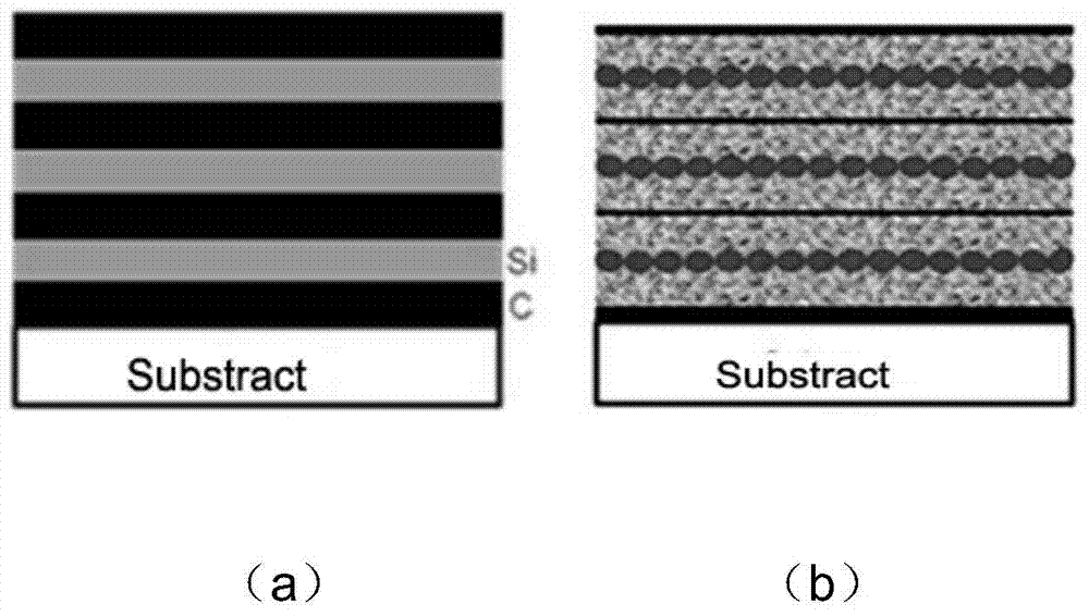
[0031] 2) Ar gas is used as the sputtering atmosphere. Under the condition of applying a bias voltage to the substrate, the silicon target and the carbon target are respectively subjected to magnetron co-sputtering by radio frequency and DC power, and amorphous silicon / silicon is alternately deposited on the glass or silicon substrate. Carbon superlattice structure multilayer film;

[0032] Among them, the method of a...

Embodiment 1

[0044] Glass is selected as the substrate and pre-treated before coating. The thickness of the substrate is 500um, and it is ultrasonically cleaned for 15 minutes by surfactant cocoic acid monoethanolamide (CMEA), (flowing) deionized water, acetone, and absolute ethanol.

[0045] Using argon as the sputtering gas, carry out magnetron co-sputtering on the silicon target and the carbon target, deposit the silicon layer and the carbon layer on the glass substrate, keep the thickness of the carbon layer at 10nm, change the thickness of the silicon layer, and make the modulation wavelength ratio 0.6 Superlattice Si / C multilayer thin film. Among them, the silicon target uses a 100W RF power supply, the carbon target uses a 100W DC power supply, and the substrate bias voltage is 80V; the sputtering Ar gas flow rate is 4 sccm; the deposition time is about 1.h, and the film thickness is about 120nm. The sample was annealed in stages under a nitrogen atmosphere: first, the temperature w...

Embodiment 2

[0049] A single crystal silicon wafer was selected as the substrate and pre-treated before coating. The thickness of the substrate was 520um, and it was ultrasonically cleaned for 20 minutes by the surfactant coconut acid diethanolamide, (flowing) deionized water, acetone, and absolute ethanol.

[0050] Using argon as the sputtering gas, carry out magnetron co-sputtering on the silicon target and the carbon target, deposit the silicon layer and the carbon layer on the single crystal silicon substrate, keep the thickness of the carbon layer at 10nm, change the thickness of the silicon layer, and make the modulated wavelength Superlattice Si / C multilayer films with a ratio of 0.7. Among them, the silicon target uses a 100W RF power supply, the carbon target uses a 100W DC power supply, and the substrate bias voltage is 80V; the sputtering Ar gas flow rate is 4 sccm; the deposition time is about 1.8h, and the film thickness is about 120nm. The sample was annealed in stages under ...


PUM

PropertyMeasurementUnit
thicknessaaaaaaaaaa
sizeaaaaaaaaaa
purityaaaaaaaaaa

Abstract

The invention relates to a preparing method of self-assembly forming-dimension-controllable silicon nanocrystal films. The method mainly comprises the following steps that firstly, after the film coating pretreatment, Ar ions are used for carrying out magnetron co-sputtering on Si targets and C targets, the sputtering powers of the Si and C targets are regulated, and amorphous silicon / carbon films of a multilayer structure are alternately deposited on a silicon and glass substrate; then, the staged annealing is carried out in the nitrogen atmosphere, and the alpha-SiC / nc-Si multilayer structure films are formed. The silicon nanocrystal dimension formed by the films is controllable in a range being 2 to 10nm, meanwhile, the density of silicon nanocrystals is also controllable, and the optical band gap of the silicon nanocrystals in the range is controllably changed in a range being 2.7 to 1.8eV. The preparing method provided by the invention has the advantages that the silicon nanocrystals with the controllable dimension and density can be formed through the superlattice structure Si / C multilayer films, further, the absorption spectrum range is regulated, and in addition, the photoelectric conversion efficiency of used materials can be obviously improved. Through the films, the light absorption range and the photoelectric conversion efficiency of silicon-based photovoltaic devices are hopeful to be greatly improved.

Description

technical field [0001] The invention belongs to the technical field of third-generation solar cells, in particular to a method for self-assembling to form a size-controllable silicon nanocrystal thin film embedded in an amorphous medium, and belongs to the technical field of solar cells and nanomaterial applications. Background technique [0002] Photovoltaic solar cells are a very important energy industry today and in the future. The third-generation solar cell is a new type of nanostructured cell, and its goal is to reduce the cost and significantly improve the photoelectric conversion efficiency of photovoltaic devices on the basis of the second-generation thin-film solar cell. Silicon nanocrystalline solar cells are representative of the third generation of solar cells. Silicon nanocrystals are embedded in amorphous silicide to form a two-phase system. Compared with amorphous silicon, its electron mobility is high and its performance is stable. The size of the optical...

Claims


Application Information

Patent Timeline
Patent Type & Authority Applications(China)
IPC IPC(8): H01L21/00H01L21/20
CPCH01L21/02527H01L21/02529H01L21/02592H01L21/02598H01L21/02631H01L31/204Y02E10/50
Inventor 畅庚榕马飞徐可为韩婷
Owner 温岭艾斯达特新材料科技有限公司
Why Eureka
Try Eureka