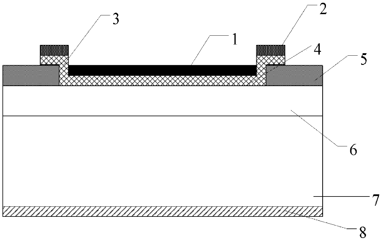
Manufacturing method of silicon carbide schottky junction type nuclear battery including niobium-doped n-type epitaxial layer
An epitaxial layer and silicon carbide technology, which is applied in the intersection of nuclear technology and microelectronics, can solve the problems of large energy loss of incident particles and low energy conversion efficiency, so as to increase the width of the depletion region, improve the collection rate, and improve the open circuit voltage. and energy conversion efficiency
- Summary
- Abstract
- Description
- Claims
- Application Information
AI Technical Summary
Problems solved by technology
Method used
Image
Examples
Embodiment 1
[0018] Step 1, epitaxial n-type epitaxial layer on SiC highly doped n-type substrate sample.
[0019] The selected doping concentration is 1×10 18 cm -3 The highly doped n-type SiC substrate 7, after cleaning, is epitaxially grown on the highly doped n-type SiC substrate with a thickness of 4um and an initial n-type epitaxial layer doped with nitrogen ions, and its doping concentration is 1×10 15 cm -3 , the epitaxy temperature is 1570°C, the pressure is 100mbar, the reaction gases are silane and propane, the flow rates are 50sccm and 150sccm respectively, the carrier gas is pure hydrogen, and the impurity source is liquid nitrogen.
[0020] Step 2: For a nitrogen doping concentration of 1 x 10 15 cm -3 The initial n-type SiC epitaxial layer is implanted with niobium ions.
[0021] (2.1) The concentration of nitrogen doping is 1×10 15 cm -3 The initial n-type SiC epitaxial layer was implanted with niobium ions, and the conditions of the niobium ion implantation were: th...
Embodiment 2
[0037] Step 1: Epitaxial n-type epitaxial layer on SiC highly doped n-type substrate sample.
[0038] The selected doping concentration is 5×10 18 cm -3 The highly doped n-type SiC substrate 7, after cleaning, is epitaxially grown on the highly doped n-type SiC substrate with a thickness of 3um and an initial n-type epitaxial layer doped with nitrogen ions, and its doping concentration is 5×10 15 cm -3 , the epitaxy temperature is 1570°C, the pressure is 100mbar, the reaction gases are silane and propane, the flow rates are 50sccm and 150sccm respectively, the carrier gas is pure hydrogen, and the impurity source is liquid nitrogen.
[0039] Step 2: The concentration of nitrogen doping is 5×10 15 cm -3 The initial n-type SiC epitaxial layer is implanted with niobium ions.
[0040] (2.1) The concentration of nitrogen doping is 5×10 15 cm -3 The initial n-type SiC epitaxial layer was implanted with niobium ions, and the conditions of the niobium ion implantation were: the e...
Embodiment 3
[0056] Step A: Epitaxial n-type epitaxial layer on SiC highly doped n-type substrate sample.
[0057] The selected doping concentration is 7×10 18 cm -3 The highly doped n-type SiC substrate 7, after cleaning, is epitaxially grown on the highly doped n-type SiC substrate with a thickness of 5um and an initial n-type epitaxial layer doped with nitrogen ions, and its doping concentration is 2×10 15 cm -3 , the epitaxy temperature is 1570°C, the pressure is 100mbar, the reaction gases are silane and propane, the flow rates are 50sccm and 150sccm respectively, the carrier gas is pure hydrogen, and the impurity source is liquid nitrogen.
[0058] Step B: For a nitrogen doping concentration of 2 x 10 15 cm -3 The initial n-type SiC epitaxial layer is implanted with niobium ions.
[0059] (B1) The concentration of nitrogen doping is 2×10 15 cm -3 The initial n-type SiC epitaxial layer was implanted with niobium ions, and the conditions of the niobium ion implantation were: the...
PUM
| Property | Measurement | Unit |
|---|---|---|
| thickness | aaaaa | aaaaa |
| thickness | aaaaa | aaaaa |
Abstract
Description
Claims
Application Information
