

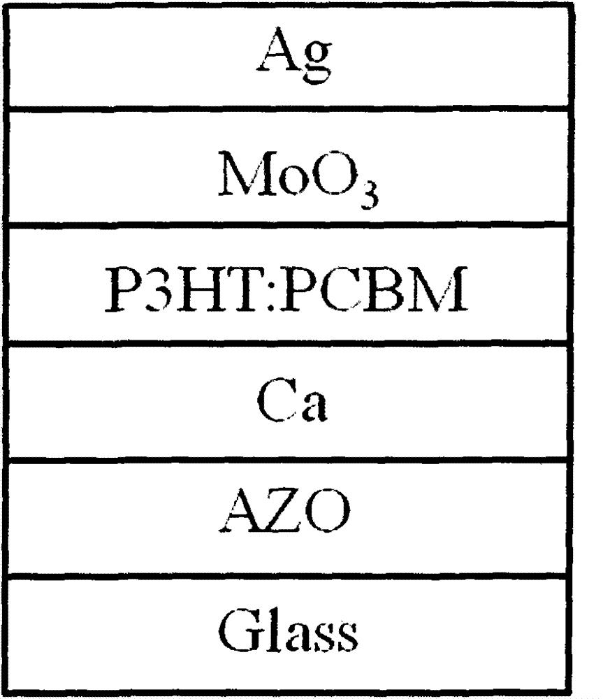
Organic solar cell based on AZO/Ca cathode and manufacturing method thereof
A solar cell and organic technology, applied in semiconductor/solid-state device manufacturing, circuits, photovoltaic power generation, etc., can solve the problems of lack of device structure and preparation technology, rare research and reports, etc., to improve short-circuit current density and fill factor, easy Large-area film formation and cost reduction effect
- Summary
- Abstract
- Description
- Claims
- Application Information
AI Technical Summary
Problems solved by technology
Method used
Image

Examples
Embodiment 1
[0037] The realization steps of the present invention are as follows:
[0038] Step 1, cleaning the substrate substrate.
[0039] The AZO glass substrate was ultrasonically cleaned in deionized water, acetone, absolute ethanol and deionized water for 15 minutes in sequence. After cleaning, it was blown dry with a nitrogen gun, and then placed in a nitrogen atmosphere glove box. The thickness of glass is about 2mm, the thickness of AZO is about 980nm, and the sheet resistance is about 10Ω / □.
[0040] Step 2, depositing a Ca electron transport layer.
[0041] Thermally evaporate the Ca-modified layer with a background vacuum of 4×10 -4 Pa, current 27A, evaporation rate 0.05nm / s, thickness 5nm;
[0042] Step 3, depositing the photoactive layer of P3HT:PCBM.
[0043]First, P3HT and PCBM were dissolved in 1-2 chlorobenzene respectively to obtain a solution with a concentration of 20 mg / mL. After stirring at room temperature for 4 hours, they were mixed at a volume ratio of 1:0....
Embodiment 2
[0054] The realization steps of the present invention are as follows:
[0055] Step 1, cleaning the substrate substrate.
[0056] The AZO glass substrate was ultrasonically cleaned in deionized water, acetone, absolute ethanol and deionized water for 15 minutes in sequence. After cleaning, it was blown dry with a nitrogen gun, and then placed in a nitrogen atmosphere glove box. The thickness of glass is about 2mm, the thickness of AZO is about 980nm, and the sheet resistance is about 10Ω / □.
[0057] Step 2, depositing a Ca electron transport layer.
[0058] Thermally evaporate the Ca-modified layer with a background vacuum of 4×10 -4 Pa, current 27A, evaporation rate 0.05nm / s, thickness 1nm;
[0059] Step 3, depositing the photoactive layer of P3HT:PCBM.
[0060] First, P3HT and PCBM were dissolved in 1-2 chlorobenzene respectively to obtain a solution with a concentration of 20 mg / mL. After stirring at room temperature for 4 hours, they were mixed at a volume ratio of 1:0...
PUM
 Abstract
Description
Claims
Application Information