Sodium doping method for CIGS-based thin film photovoltaic material
A thin-film photovoltaic and sodium-doped technology, which is applied in photovoltaic power generation, sustainable manufacturing/processing, electrical components, etc., can solve problems such as spots, affecting appearance, and weak bonding between Mo electrode layer and CIGS light-absorbing layer. achieve the effect of avoiding poisoning
- Summary
- Abstract
- Description
- Claims
- Application Information
AI Technical Summary
Problems solved by technology
Method used
Image

Examples
Embodiment 1
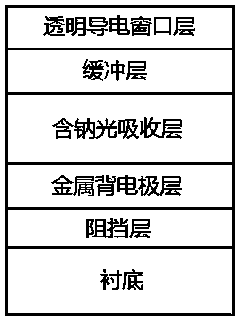
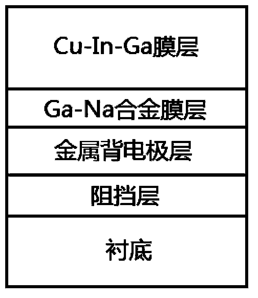
[0028] On a substrate made of soda-lime glass, magnetron sputtering is used to deposit a 50nm silicon oxide film layer; then a metal molybdenum electrode layer of 800 nm is deposited on the silicon oxide film layer by magnetron sputtering; The sodium gallium alloy film layer and the copper indium gallium metal prefabricated layer are sequentially deposited by controlled sputtering, so that the total thickness of the gallium sodium alloy film layer and the copper indium gallium metal prefabricated layer is 1.2um, and gallium containing 70at%Ga and 30at%Na is used The sodium alloy target is sputtered to deposit the sodium gallium alloy film layer; then it is put into a heating furnace for selenization heat treatment, thereby forming a copper indium gallium diselenide sodium-containing optical absorption layer with a chalcopyrite structure; A 40nm CdS film was deposited on the absorber layer as a buffer layer by the chemical bath (CBD) method; a 40nm intrinsic ZnO film was deposit...
Embodiment 2
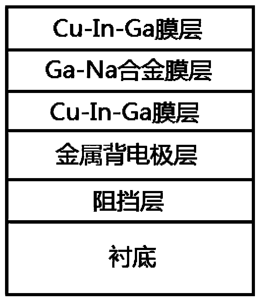
[0039] A 20nm titanium oxide film layer was deposited by magnetron sputtering on a substrate of soda lime glass; then a metal molybdenum electrode layer of 800nm was deposited on the titanium oxide film layer by magnetron sputtering; The copper indium gallium metal prefabricated layer, the gallium sodium alloy film layer, and the copper indium gallium metal prefabricated layer are sequentially deposited by controlled sputtering, so that the total thickness of the gallium sodium alloy film layer and the copper indium gallium metal prefabricated layer is 1.2um, and the gallium-containing 80at% Ga and 20at% Na gallium sodium alloy target is sputtered to deposit gallium sodium alloy film layer; then it is put into a heating furnace for selenization heat treatment to form copper indium gallium diselenide containing sodium light with chalcopyrite structure Absorbing layer; a 40nm CdS film was deposited on the sodium-containing light absorbing layer by the chemical bath (CBD) method...
Embodiment 3
[0042] A 20nm zirconia film layer was deposited by magnetron sputtering on a substrate of soda lime glass; then a 50nm metal molybdenum electrode layer with tensile stress was deposited on the zirconia film layer by magnetron sputtering, and then deposited A layer of 500nm metal molybdenum electrode layer with compressive stress, the metal back electrode layer is composed of double-layer molybdenum electrode layers; then magnetron sputtering is used to sequentially deposit copper indium gallium metal prefabricated layer and gallium sodium alloy film on the metal back electrode layer layer, so that the total thickness of the sodium gallium alloy film layer and the copper indium gallium metal prefabricated layer is 1.2um, and the sodium gallium alloy film layer is deposited by sputtering with a sodium gallium alloy target material containing gallium 62at%Ga and 38at%Na; Put it into a heating furnace for selenization heat treatment to form a copper indium gallium diselenide sodium...
PUM
| Property | Measurement | Unit |
|---|---|---|
| Thickness | aaaaa | aaaaa |
| Grain size | aaaaa | aaaaa |
| Grain size | aaaaa | aaaaa |
Abstract
Description
Claims
Application Information
 - R&D
- Intellectual Property
- Life Sciences
- Materials
- Tech Scout
- Unparalleled Data Quality
- Higher Quality Content
- 60% Fewer Hallucinations
Browse by: Latest US Patents, China's latest patents, Technical Efficacy Thesaurus, Application Domain, Technology Topic, Popular Technical Reports.
© 2025 PatSnap. All rights reserved.Legal|Privacy policy|Modern Slavery Act Transparency Statement|Sitemap|About US| Contact US: help@patsnap.com