4H-SiC metal semiconductor field-effect transistor

A field-effect transistor and metal-semiconductor technology, applied in the field of field-effect transistors, can solve problems such as lattice damage, limited improvement range, and decrease in effective carrier mobility.

Inactive Publication Date: 2014-07-16
XIDIAN UNIV
View PDF3 Cites 10 Cited by
  • Summary
  • Abstract
  • Description
  • Claims
  • Application Information

AI Technical Summary

Problems solved by technology

[0004] Compared with the double-recessed structure, although the breakdown voltage of the above-mentioned recessed source / drain drift region 4H-SiC MESFET increases due to the reduction of the thickness of the drift region between the gate and drain, the improvement is limited.
And in practice, the process of reactive ion etching (RIE) will form lattice damage on the surface of the drift region of the device, resulting in a decrease in the effective mobility of carriers in the N-type channel layer, thereby reducing the drain current. In terms of current output characteristics manifested as a degradation of the saturation current

Method used


Image

  • 4H-SiC metal semiconductor field-effect transistor
  • 4H-SiC metal semiconductor field-effect transistor

Examples


Embodiment 1

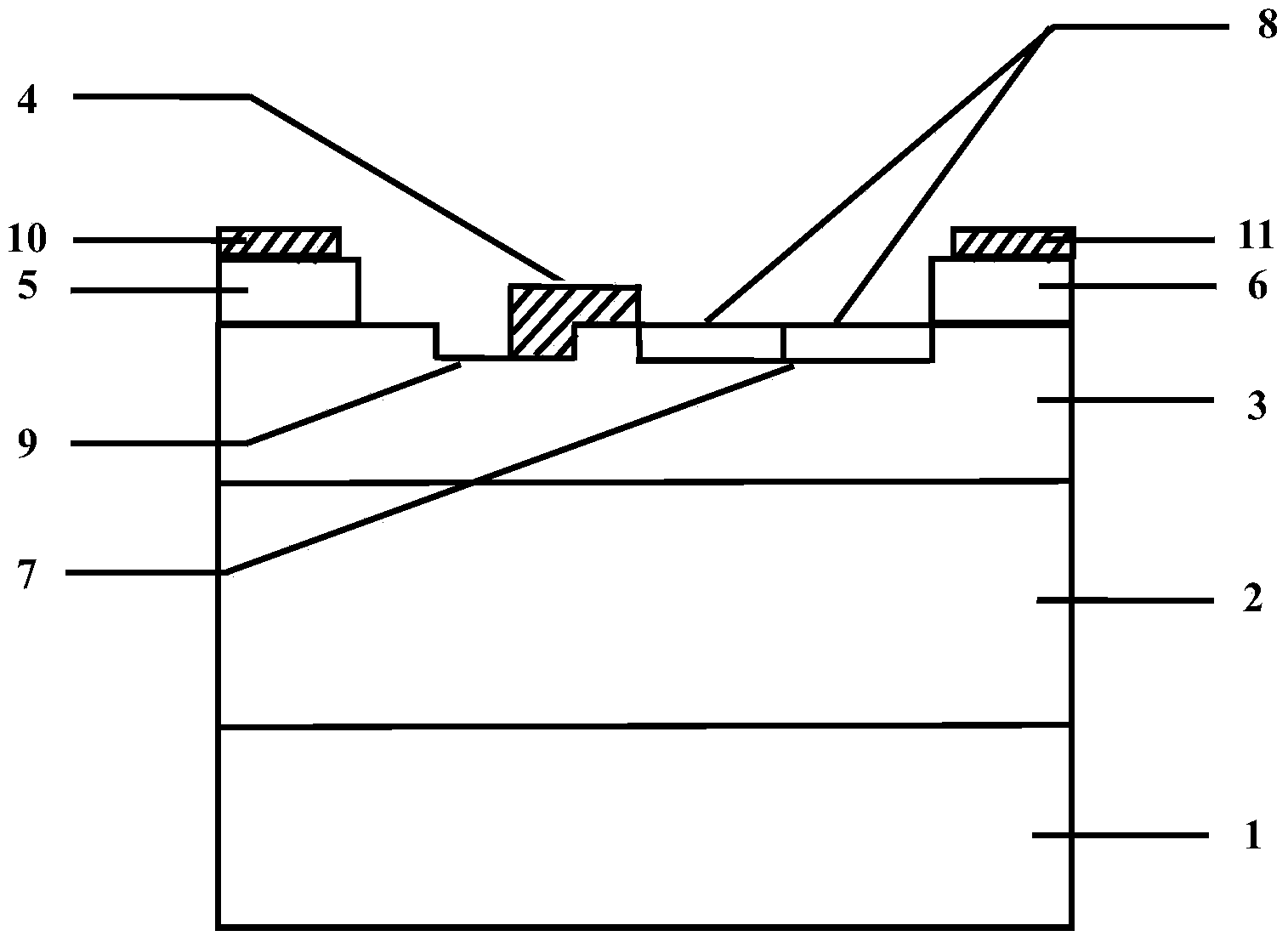
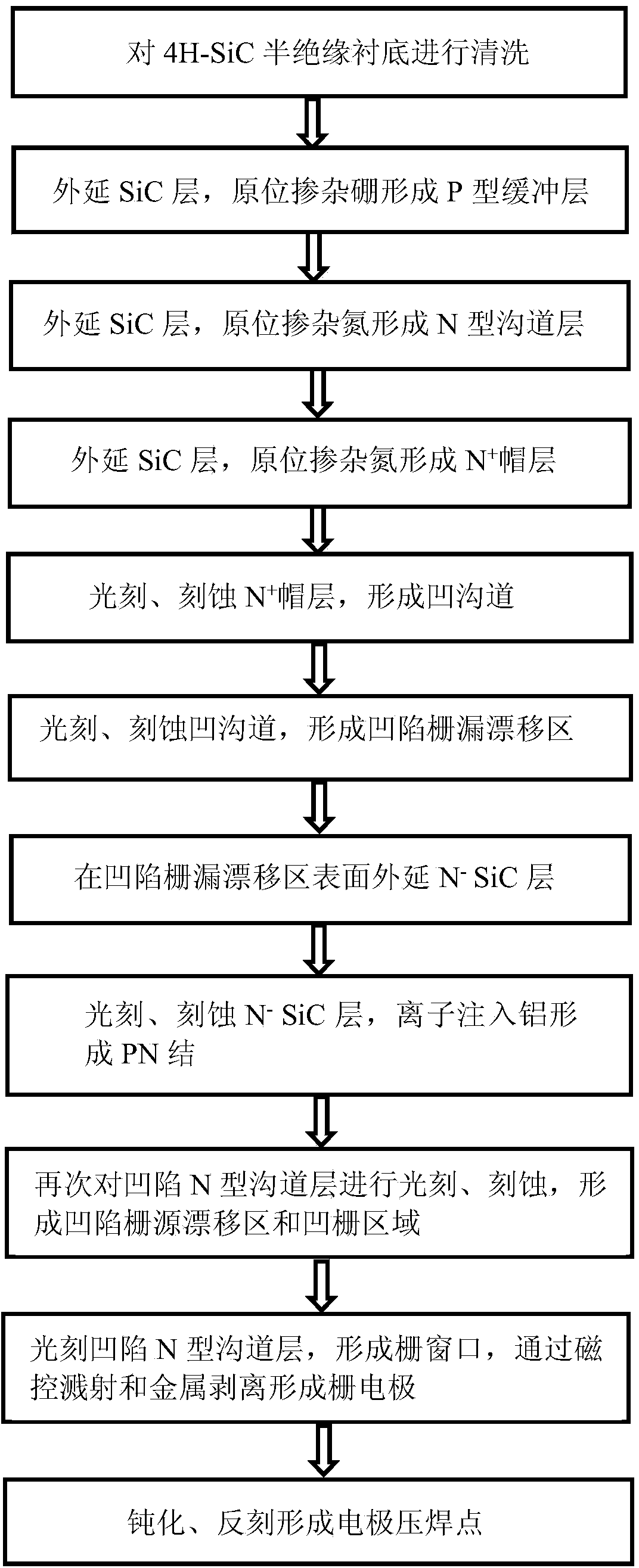
[0036] Example 1: Fabrication of a 4H-SiC metal semiconductor field effect transistor containing a PN junction with a thickness of 0.04 μm and a P region length of 0.45 μm.

[0037] The manufacturing steps of this embodiment are as follows:

[0038] Step 1: Clean the 4H-SiC semi-insulating substrate to clean the surface.

[0039] (1.1) Carefully clean the substrate twice with a cotton ball dipped in methanol;

[0040] (1.2) Wash the substrate in xylene at 80°C, boiled acetone and methanol at 80°C for 4 minutes, and then dry it with dry high-purity nitrogen;

[0041] (1.3) Put the substrate in H 2 SO 4 With H 2 O 2 After immersing in the mixture with a ratio of 1:1 for 10 minutes, rinse with deionized water twice, and finally dry the substrate with nitrogen.

[0042] Step 2: Epitaxially grow a SiC layer on the surface of the 4H-SiC semi-insulating substrate, and form a P-type buffer layer by boron in-situ doping.

[0043] Put the 4H-SiC semi-insulating substrate into the growth chamber, an...

Embodiment 2

[0076] Example 2: Fabrication of a 4H-SiC metal semiconductor field effect transistor containing a PN junction with a thickness of 0.05 μm and a P region length of 0.5 μm.

[0077] The manufacturing steps of this embodiment are as follows:

[0078] Step 1: Same as Step 1 of Example 1.

[0079] Step 2: Same as Step 2 of Example 1.

[0080] Step 3: Same as Step 3 of Example 1.

[0081] Step 4: Same as Step 4 of Example 1.

[0082] Step 5: Same as Step 5 of Example 1.

[0083] Step 6: Same as Step 6 of Example 1.

[0084] Step 7: Same as Step 7 of Example 1.

[0085] Step 8: Same as Step 8 of Example 1.

[0086] Step 9: Epitaxy N on the surface of the recessed gate-drain drift region ‐ SiC layer.

[0087] In the growth chamber, flow of 20ml / min of silane, 10ml / min of propane, 80l / min of high-purity hydrogen and 2ml / min of high-purity nitrogen were simultaneously introduced. The growth temperature was 1550℃ and the pressure was 10 5 Continue for 36s under Pa conditions and grow 0.05μm thick N ‐...

Embodiment 3

[0094] Example 3: Fabrication of a 4H-SiC metal semiconductor field effect transistor containing a PN junction with a thickness of 0.045 μm and a P region length of 0.48 μm.

[0095] The manufacturing steps of this embodiment are as follows:

[0096] Step A: Same as Step 1 of Example 1.

[0097] Step B: Same as Step 2 of Example 1.

[0098] Step C: Same as Step 3 of Example 1.

[0099] Step D: Same as Step 4 of Example 1.

[0100] Step E: Same as Step 5 of Example 1.

[0101] Step F: Same as Step 6 of Example 1.

[0102] Step G: Same as Step 7 of Example 1.

[0103] Step H: Same as Step 8 of Example 1.

[0104] Step I: Epitaxy N on the surface of the recessed gate-drain drift region ‐ SiC layer.

[0105] In the growth chamber, flow of 20ml / min of silane, 10ml / min of propane, 80l / min of high-purity hydrogen and 2ml / min of high-purity nitrogen were simultaneously introduced. The growth temperature was 1550℃ and the pressure was 10 5 Continue for 33s under Pa conditions, grow 0.045μm thick N ‐...


PUM


Abstract

The invention discloses a 4H-SiC metal semiconductor field-effect transistor. The 4H-SiC metal semiconductor field-effect transistor mainly solves the problems that in the prior art, output current of a drain electrode is unstable, and breakdown voltage is low. The 4H-SiC metal semiconductor field-effect transistor structurally comprises a 4H-SiC semi-insulating substrate (1), a P-type buffer layer (2) and an N-type channel layer (3) from bottom to top, wherein a source electrode cap layer (5) and a drain electrode cap layer (6) are arranged on the surface of the N-type channel layer (3), a source electrode (10) and a drain electrode (11) are arranged on the surface of the source electrode cap layer (5) and the surface of the drain electrode cap layer (6) respectively, a gate electrode (4) is formed on one side of the portion, close to the source electrode cap layer (5), of the top of the N-type channel layer (3), a sunken gate source drift region (9) is formed between the gate electrode (4) and the source electrode cap layer (5), a sunken gate drain drift region (7) is formed between the gate electrode (4) and the drain electrode cap layer (6), and transverse PN junctions (8) are arranged on the surface of the sunken gate drain drift region (7). The 4H-SiC metal semiconductor field-effect transistor has the advantages that the breakdown voltage is high, and the output current of the drain electrode is stable.

Description

Technical field [0001] The invention relates to the technical field of electronic components, in particular to a field effect transistor, which can be applied as a high-power semiconductor device. Background technique [0002] SiC material has excellent electrical and material properties such as wide band gap, large critical breakdown electric field, high electron saturation rate, and high thermal conductivity, which determines that it is a semiconductor microwave power device, especially in the production of metal semiconductor field effect transistors (MESFET) An inevitable trend of Among the multiple homogeneous polytypes of SiC, the electron mobility of the hexagonal close-packed wurtzite structure 4H-SiC is about twice that of the same structure 6H-SiC, so most power devices use 4H-SiC as the manufacturing material. With the growth of military and commercial demand for high-power devices, there is an increasing need to increase the breakdown voltage and output power of 4H-S...

Claims


Application Information

Patent Timeline
Patent Type & Authority Applications(China)
IPC IPC(8): H01L29/78H01L29/06H01L21/336
CPCH01L29/0619H01L29/66068H01L29/812H01L29/8128
Inventor 贾护军裴晓延孙哲霖
Owner XIDIAN UNIV
Why Eureka
Try Eureka