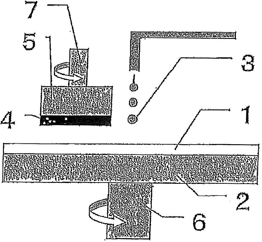
Polishing pad

A polishing pad and polyurethane resin technology, applied in the field of polishing pads, can solve problems such as scratches on polishing materials, and achieve the effects of excellent flattening properties, large wear parameters, and excellent dressability.

Inactive Publication Date: 2014-07-30
ROHM & HAAS ELECTRONICS MATERIALS CMP HLDG INC
View PDF10 Cites 7 Cited by
  • Summary
  • Abstract
  • Description
  • Claims
  • Application Information

AI Technical Summary

Problems solved by technology

[0009] However, if polymerized diisocyanate is used, the hardness of the polyurethane resin foam becomes high, and if a polishing pad containing the polyurethane resin foam is used, scratches tend to be easily generated on the surface of the material to be polished.

Method used


Image

  • Polishing pad
  • Polishing pad
  • Polishing pad

Examples


Embodiment 1

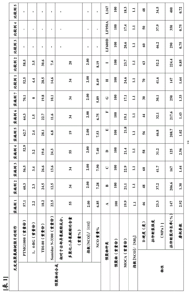
[0137] (Production of non-foamed polyurethane resin sheet)

[0138] 18.2 parts by weight of toluene diisocyanate (manufactured by Mitsui Chemicals, TDI-80, a mixture of 2,4-isomer / 2,6-isomer=80 / 20), 22.5 parts by weight of multimerization 1 , 6-hexamethylene diisocyanate (Sumidur N-3300, isocyanurate type, manufactured by Sumika Bayer Urethane Co., Ltd.), 57.1 parts by weight of polytetramethylene ether glycol (manufactured by Mitsubishi Chemical Corporation, PTMG1000, hydroxyl Value: 112.2KOHmg / g), 2.2 parts by weight of 1,4-butanediol (manufactured by NACALAI Chemical Co., Ltd., 1,4-BG), and reacted at 70° C. for 4 hours to obtain an isocyanate-terminated prepolymer A. Moreover, content of polymerized 1, 6- hexamethylene diisocyanate was 55 weight% with respect to the whole isocyanate component.

[0139] Add 100 parts by weight of the prepolymer A and 19.9 parts by weight of 4,4'-methylene bis(o-chloroaniline) melted at 120°C to a planetary stirring defoaming device for def...

Embodiment 2-7、 comparative example 1-5

[0144] A non-foaming polyurethane resin sheet and a polishing pad were produced in the same manner as in Example 1 except that the compounding quantities described in Table 1 and Table 2 were used. The compounds in Table 1 and Table 2 are described below.

[0145] LF600D: manufactured by Chemtura, a prepolymer synthesized from toluene diisocyanate and polytetramethylene ether glycol, NCO wt% = 7.25

[0146] LF950A: manufactured by Chemtura, a prepolymer synthesized from toluene diisocyanate and polytetramethylene ether glycol, NCO wt% = 6.05

[0147] L167: manufactured by Chemtura, a prepolymer synthesized from toluene diisocyanate and polytetramethylene ether glycol, NCO wt% = 6.30
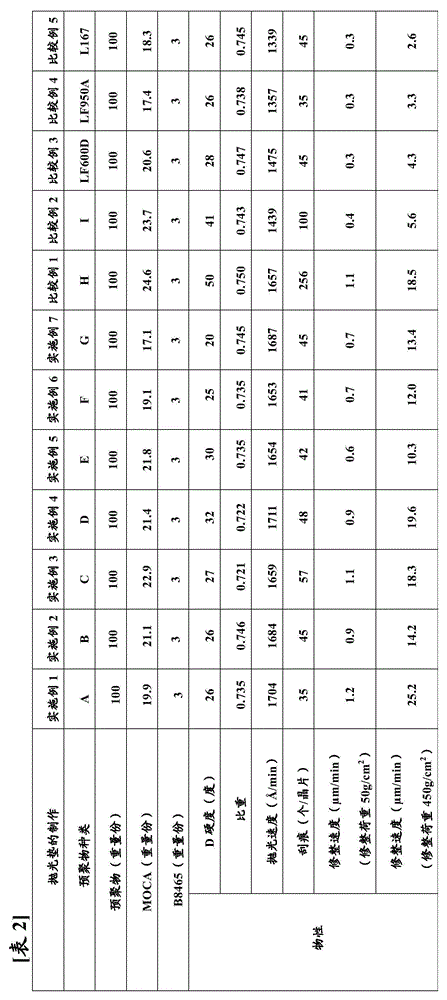
[0148]

[0149]

Embodiment 8

[0151] (Manufacturing of polishing pads)

[0152] 100 parts by weight of the prepolymer F, 3 parts by weight of a silicon-based surfactant (manufactured by Goldschmidt, B8465) and 0.75 parts by weight of a tertiary amine catalyst (manufactured by Kao Company, KAO: No25 (N,N-dimethylamino Hexanol)) was added into the polymerization container, mixed, adjusted to 80° C., and degassed under reduced pressure. Then, vigorously stirred at 900 rpm using a stirring blade for about 4 minutes so as to introduce air bubbles into the reaction system. 19.1 parts by weight of 4,4'-methylenebis(o-chloroaniline) previously melted at 120° C. was added thereto. After stirring this liquid mixture for about 1 minute, it poured into the flat-bottomed open mold (injection molding container). When the fluidity of the liquid mixture disappeared, it was placed in an oven, and post-cured at 100° C. for 16 hours to obtain a polyurethane resin foam block.

[0153] The polyurethane resin foam block heat...


PUM

PropertyMeasurementUnit
hardnessaaaaaaaaaa
diameteraaaaaaaaaa
hardnessaaaaaaaaaa

Abstract

An aim of the present invention is to provide a polishing pad which generates almost no scratches on the surface of an object to be polished, and has improved dressability. Another aim of the present invention is to provide a semiconductor device manufacturing method using the polishing pad. The polishing pad according to the present invention comprises a polishing layer formed of a microbubble-containing polyurethane resin foam. The polyurethane resin foam contains a polyurethane resin whose asker D hardness is between 20 degrees and 60 degrees, and whose wear parameter, which is expressed by the following formula, is between 1 and 3. Wear parameter = {1 / (tensile breaking strength [MPa] tensile breaking elongation [%] / 100)} 100

Description

technical field [0001] The present invention relates to a polishing pad capable of stably and efficiently polishing optical materials such as lenses and mirrors, silicon wafers, glass substrates for hard disks, aluminum substrates, and general metal polishing processes requiring a high degree of surface flatness Perform flattening processing. The polishing pad of the present invention is particularly suitable for the step of planarizing silicon wafers and devices on which oxide layers, metal layers, etc. are formed, before lamination and formation of these oxide layers or metal layers. Background technique [0002] As a representative material requiring a high degree of surface flatness, a single-crystal silicon wafer called a silicon wafer for manufacturing semiconductor integrated circuits (IC, LSI) can be cited. In the manufacturing steps of IC, LSI, etc., in order to form reliable semiconductor connection of various thin films used to form circuits on silicon wafers, it...

Claims


Application Information

Patent Timeline
Patent Type & Authority Applications(China)
IPC IPC(8): B24B37/24C08G18/00H01L21/304
CPCB24B37/24C08G18/12C08G18/3206C08G18/4854C08G18/6674C08G18/725C08G18/7621C08G18/792C08G2110/0008C08G18/3808B24D11/001H01L21/304
Inventor 清水绅司
Owner ROHM & HAAS ELECTRONICS MATERIALS CMP HLDG INC
Why Eureka
Try Eureka