Gallium-doped polycrystalline silicon ingot and preparation method thereof
A technology of polycrystalline silicon ingots and molten silicon, which is applied in the field of gallium-doped polycrystalline silicon ingots and its preparation, can solve the problems of lower battery conversion efficiency, low ingot yield, light-induced attenuation, etc., to avoid deterioration of battery efficiency and high photoelectric conversion efficiency , the effect of uniform resistivity distribution
- Summary
- Abstract
- Description
- Claims
- Application Information
AI Technical Summary
Problems solved by technology
Method used
Image

Examples
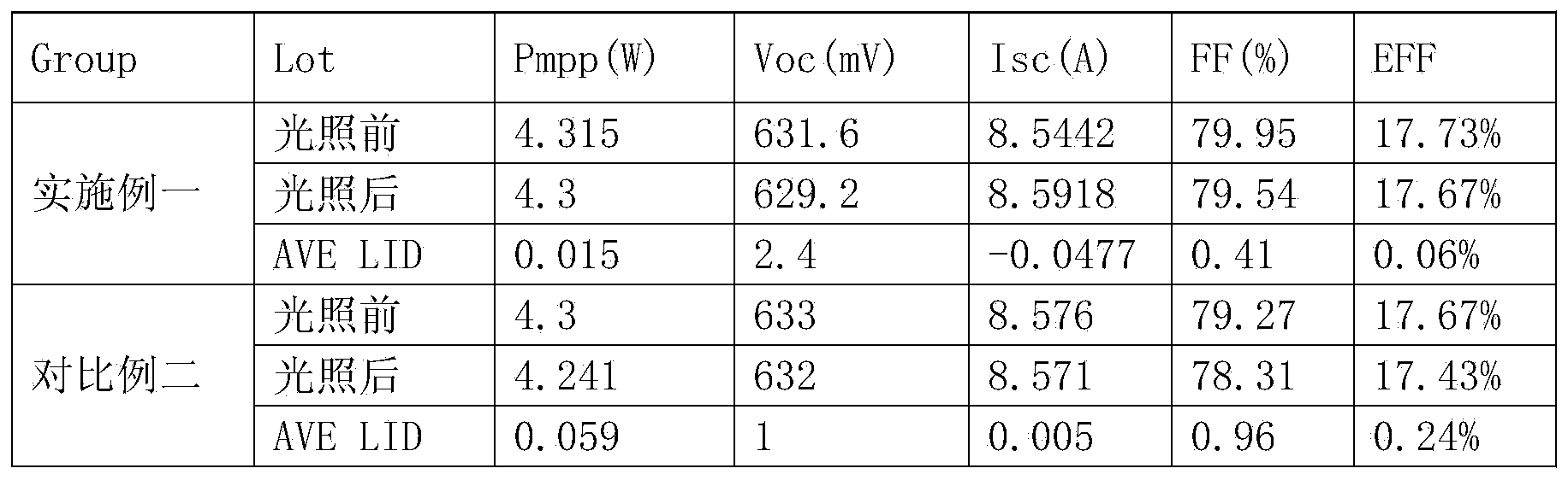
Embodiment 1
[0031] A preparation method for a gallium-doped polycrystalline silicon ingot, comprising the steps of:
[0032] (1) coating a silicon nitride coating on the inner wall of the crucible; the thickness of the silicon nitride coating is 60 microns, and its purity is greater than 99.9%;
[0033] (2) polysilicon material and gallium dopant are loaded into the crucible to form a mixture;
[0034] The gallium dopant is located in the area of 30% to 50% of the height of the crucible; the content of gallium in silicon in the mixture is 6ppma;
[0035] (3) Put the crucible containing the mixture into the ingot casting furnace, evacuate it, and then heat it at a temperature of 1500-1550°C, so that the mixture is gradually melted in order from top to bottom;
[0036] When the gallium dopant in the mixture starts to melt, adjust the furnace pressure so that the furnace pressure is 700-800mbar;
[0037] Enter the crystal growth stage immediately after the mixture is completely melted to...
PUM
| Property | Measurement | Unit |
|---|---|---|
| thickness | aaaaa | aaaaa |
| thickness | aaaaa | aaaaa |
| purity | aaaaa | aaaaa |
Abstract
Description
Claims
Application Information
 - R&D
- Intellectual Property
- Life Sciences
- Materials
- Tech Scout
- Unparalleled Data Quality
- Higher Quality Content
- 60% Fewer Hallucinations
Browse by: Latest US Patents, China's latest patents, Technical Efficacy Thesaurus, Application Domain, Technology Topic, Popular Technical Reports.
© 2025 PatSnap. All rights reserved.Legal|Privacy policy|Modern Slavery Act Transparency Statement|Sitemap|About US| Contact US: help@patsnap.com