Epitaxial wafer of gan-based light-emitting diode and manufacturing method thereof
A technology of light-emitting diodes and epitaxial wafers, applied in the direction of electrical components, circuits, semiconductor devices, etc., can solve the problems of lowering the effective barrier of EBL, reducing the luminous efficiency of light-emitting diodes, lattice mismatch and enhancement of polarization effects, etc., to achieve enhanced Anti-static breakdown ability, avoiding lattice mismatch defects, and improving injection efficiency
- Summary
- Abstract
- Description
- Claims
- Application Information
AI Technical Summary
Problems solved by technology
Method used
Image
Examples
Embodiment 1
[0029] An embodiment of the present invention provides a schematic structural diagram of an epitaxial wafer of a GaN-based light-emitting diode, see figure 1 , the epitaxial wafer includes: the epitaxial wafer includes a substrate 1, a buffer layer 2 grown on the substrate 1, an N-type gallium nitride layer 4, a multi-quantum well layer 5 and a P-type gallium nitride layer 6, and the multi-quantum well Layer 5 is a superlattice structure, and the superlattice structure includes alternately grown quantum well layers 51 and quantum barrier layers 52. Composite layer 7, composite layer 7 includes a plurality of cycles, composite layer 7 in each cycle includes insertion layer 71 and electron blocking layer 72, starting from the side of multi-quantum well layer 5, insertion layer 71 and electron blocking layer 72 are stacked sequentially Arranged, the insertion layer 71 is an Al-doped zinc oxide (ZnO) layer.
[0030] The insertion layer of the ZnO layer doped with Al element has a...
Embodiment 2
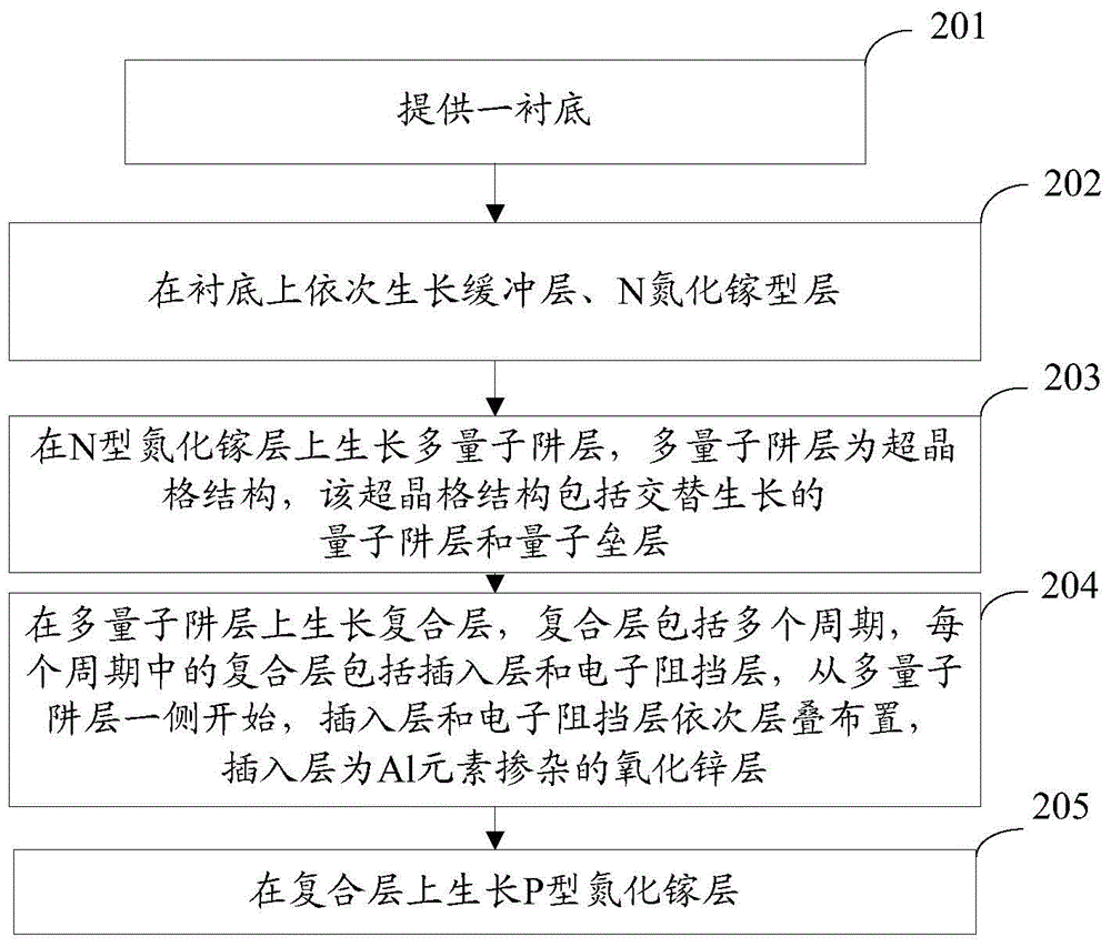
[0047] An embodiment of the present invention provides a method for fabricating an epitaxial wafer of a GaN-based light-emitting diode, see figure 2 , methods include:
[0048] Step 201: Provide a substrate.
[0049] In this embodiment, the substrate includes but not limited to a sapphire substrate.
[0050] During implementation, the substrate can be placed in H at 1000-1200°C 2 The heat treatment is carried out under the atmosphere for 8 minutes to clean the surface, and then the substrate is nitrided.
[0051] Step 202: growing a buffer layer and an N-type gallium nitride layer sequentially on the substrate.
[0052] Wherein, the buffer layer may include a low-temperature buffer layer and a high-temperature buffer layer.
[0053] Optionally, the low-temperature buffer layer may be a gallium nitride layer, or may be an aluminum nitride layer or an aluminum gallium nitride layer. Specifically, lower the temperature in the reaction chamber to 400-600° C., and grow a low-...
PUM
| Property | Measurement | Unit |
|---|---|---|
| thickness | aaaaa | aaaaa |
| temperature | aaaaa | aaaaa |
| thickness | aaaaa | aaaaa |
Abstract
Description
Claims
Application Information

