Right side illuminated Si-PIN photoelectric detector taking micro-nano structural silicone as light-sensitive layer and preparation method thereof

A micro-nano structure and photodetector technology, applied in the field of photoelectric detection, can solve the problems of poor thermomechanical properties, poor crystal quality, and incompatibility, and achieve the effects of high absorption rate, low cost, and high responsivity.

Inactive Publication Date: 2014-09-24
UNIV OF ELECTRONICS SCI & TECH OF CHINA
View PDF4 Cites 9 Cited by
  • Summary
  • Abstract
  • Description
  • Claims
  • Application Information

AI Technical Summary

Problems solved by technology

However, InGaAs semiconductor materials have disadvantages such as high price, poor thermomechanical properties, poor crystal quality, and not easy to be compatible with existing silicon microelectronics processes.

Method used


Image

  • Right side illuminated Si-PIN photoelectric detector taking micro-nano structural silicone as light-sensitive layer and preparation method thereof
  • Right side illuminated Si-PIN photoelectric detector taking micro-nano structural silicone as light-sensitive layer and preparation method thereof

Examples


Embodiment 1

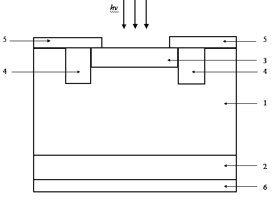
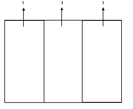
[0036] The structure of a kind of positively illuminated Si-PIN photodetector with micro-nano structure silicon as the photosensitive layer of the present invention is as follows: figure 1 As shown, it includes I-type substrate 1, N region 2, micro-nanostructure silicon layer P region 3, P + Area 4, upper metal electrode 5 and lower metal electrode 6, I-type substrate 1 can use high-resistance Si single wafer; N area 2 can be doped by phosphorus diffusion or ion implantation; micro-nano structure silicon layer P area 3 can use boron Diffusion or ion implantation doping, on which nanoimprint etching is performed; P + Region 4 can be doped with boron re-diffusion or ion implantation; the upper electrode 5 can use P-type ohmic contact; the lower electrode 6 can use N-type ohmic contact; the new Si-PIN photodetector made in this way has a micro-nano structure silicon layer and The protective ring has the characteristics of high responsivity and broad near-infrared spectral respon...


PUM


Abstract

The present invention discloses a right side illuminated Si-PIN photoelectric detector taking the micro-nano structural silicone as a light-sensitive layer and a preparation method thereof. The right side illuminated Si-PIN photoelectric detector taking the micro-nano structural silicone as the light-sensitive layer comprises an I-type substrate, an N area located under the I-type substrate, a micro-nano structural layer P area located in the center of the upper part of the I-type substrate, P+ areas located at the two sides of the upper part of the I-type substrate, upper-end electrodes located on the upper surface of the I-type substrate and a lower-end electrode located on the lower surface of an N area. Compared with the conventional Si photoelectric detector, the right side illuminated Si-PIN photoelectric detector taking the micro-nano structural silicone as the light-sensitive layer of the present invention has a higher responsivity, also can detect the near infrared light, is simple in preparation technology, and is compatible with a conventional silicon semiconductor technology.

Description

technical field [0001] The invention belongs to the technical field of photoelectric detection, and relates to the structure of a photoelectric detection device, in particular to a front-illuminated Si-PIN photodetector with micro-nano structured silicon as a photosensitive layer and a preparation method thereof. Background technique [0002] As an important part of optical fiber communication systems, infrared imaging systems, laser alarm systems and laser ranging systems, photoelectric detectors are widely used in civilian applications. At present, widely used photodetectors mainly include Si-based photodetectors and InGaAs near-infrared photodetectors. Among them, Si-PIN photodetectors have fast response speed and high sensitivity, and Si materials are easy to purify, easy to dope, rich in resources, low in cost, easy to large-scale integration and mature related technologies, so they are widely used. However, due to the large forbidden band width of Si material (1.12 eV...

Claims


Application Information

Patent Timeline
Patent Type & Authority Applications(China)
IPC IPC(8): H01L31/028H01L31/0352H01L31/105H01L31/18
CPCH01L31/028H01L31/035209H01L31/105H01L31/1804Y02P70/50
Inventor 李伟渠叶君吴程呈钟豪蒋亚东
Owner UNIV OF ELECTRONICS SCI & TECH OF CHINA
Why Eureka
Try Eureka