

Heat-resistant organic semiconductor
An organic and organic compound technology, applied in the field of heat-resistant organic semiconductor materials, can solve problems such as poor solubility and difficult film formation
- Summary
- Abstract
- Description
- Claims
- Application Information
AI Technical Summary
Problems solved by technology
Method used
Image

Examples
Embodiment 1
[0105] Example 1: Synthesis of compound (2) and compound (16).
[0106] (1) Synthesis of compound SM1
[0107]
[0108] Step1: Synthesis of compound TM1:
[0109] Weigh (14.8g, 40mmol) of 2,7-dibromophenanthrenequinone, (9.2g, 44mmol) of dipropiophenone in a 500ml three-neck flask, measure 200mL of methanol into the flask, add 2.5g of KOH, and heat up Reaction at 50° C. for 1 h, vacuum filtration to remove the solvent to obtain a gray-green solid, put into an oven and dry to obtain 18.0 g of product, yield = 82.4%;
[0110] Step2: Synthesis of compound TM2:
[0111] Weigh (3.0g, 40mmol) TM1, (0.6g, 6.1mmol) trimethylsilylacetylene 250ml three-neck flask, measure 20mL xylene in the flask, heat up to reflux, continue stirring overnight, and concentrate under reduced pressure To dryness, separated and purified by silica gel column chromatography to obtain 1.2 grams of product, yield = 35%;
[0112] Step3: Synthesis of compound SM1:
[0113] Weigh (0.9g, 1.5mmol) of TM2...
Embodiment 2
[0120] Example 2: Synthesis of compound (11), compound (36) and compound (36).
[0121] (1) Synthesis of compound SM2:
[0122]
[0123] Step1: Synthesis of compound TM1:
[0124] Weigh (21.2g, 60mmol) 2,7-dibromophenanthrenequinone, (13.2g, 66mmol) dipropiophenone in a 500ml three-neck flask, measure 300mL of methanol into the flask, add 3.7g of KOH, and heat up Reaction at 50°C for 1 h, vacuum filtration to remove the solvent to obtain a gray-green solid, put into an oven to dry to obtain 30 g of product, yield = 85%;
[0125] Step2: Synthesis of compound TM2:
[0126] Weigh (12g, 22mmol) TM1, (2.4g, 24.5mmol) trimethylsilylacetylene 250ml three-neck flask, measure 90mL xylene in the flask, heat up to reflux, continue stirring overnight, and concentrate under reduced pressure to Dry, separate and purify by silica gel column chromatography to obtain 4.3 grams of product, yield=32%;
[0127] Step3: Synthesis of compound SM2:
[0128] Weigh (4.3g, 7mmol) of TM2 into...
Embodiment 3
[0140] Embodiment 3: device application example.
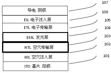
[0141] OLED preparation and comparison: in a background vacuum up to 10 -5 Pa's multi-source evaporation OLED preparation equipment adopts the following device structure: ITO / mTDATA (100 ?) / HTL (400 ?) / Host: 5% luminescent dopant 6% (300 ?) / TPBi (300 ?) / LiF(10 ?) / Al, using different HTL or different blue-emitting dopant OLED light-emitting devices for comparison. Wherein the vacuum deposition speed of each organic layer and electrode is listed in Table 2 at time.
[0142] Table 2: Preparation conditions of OLED devices (doping wt concentration in the light-emitting layer is 9%)
[0143] 。
[0144] Table 3: OLED device performance (1000 Cd / cm 2 )
[0145]
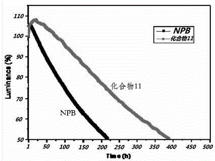
[0146] Table 3 shows that in the green triplet OLED (device B) as an example of compound 11 of the present invention, the HTL used as the hole transport layer is higher than that of the green OLED (device A) using classical NPB as the HTL at 2000 nits 70 o In t...
PUM
 Abstract
Description
Claims
Application Information