High conversion efficiency anti-pid crystalline silicon solar cell and manufacturing method thereof

A technology of solar cells and conversion efficiency, applied in the direction of final product manufacturing, sustainable manufacturing/processing, circuits, etc., can solve the high requirements of equipment furnace tube cleanliness, the increase in the proportion of defective cell appearance, and the reduction in cell conversion efficiency, etc. It can eliminate the PID effect, improve the conversion efficiency, and improve the absorption capacity.

Active Publication Date: 2017-04-26
镇江市电器设备厂有限公司
View PDF4 Cites 0 Cited by
  • Summary
  • Abstract
  • Description
  • Claims
  • Application Information

AI Technical Summary

Problems solved by technology

[0004] 1. Dry oxygen oxidation requires additional expensive equipment, and has high requirements on the cleanliness of the furnace tube of the equipment, and requires an additional process, which is more complicated;
[0005] 2. Both ozone oxidation and ultraviolet light irradiation require additional equipment. Although the process is simple, it is easy to cause a large increase in the proportion of bad appearance of the cells;
[0006] 3. Dinitrogen monoxide oxidation only needs to be integrated in the coating process, no additional equipment is required, and the process is simple, but the conversion efficiency of pure nitrous oxide oxidation to produce anti-PID cells is slightly reduced

Method used


Image

  • High conversion efficiency anti-pid crystalline silicon solar cell and manufacturing method thereof
  • High conversion efficiency anti-pid crystalline silicon solar cell and manufacturing method thereof
  • High conversion efficiency anti-pid crystalline silicon solar cell and manufacturing method thereof

Examples


Embodiment 1

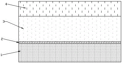
[0024] Step 1, preheating, the silicon wafer enters the reaction chamber of the tubular coating equipment, and nitrogen and ammonia gas are introduced. The flow rate of nitrogen gas is 3000 sccm / min, and the flow rate of ammonia gas is 3000 sccm / min. Turn on the radio frequency power supply to carry out the treatment of graphite boat and silicon wafer. Heating, the RF power is 5800W, the pressure range is 1.0 is Torr, the time is 240sec, and the temperature is 410℃;

[0025] Step 2, silicon oxide film layer deposition, feed nitrous oxide gas, the gas flow rate is 5000sccm / min, the pressure is 1.0Torr, the deposition time is 160sec, and a layer of silicon oxide film with a thickness of 2-3nm is deposited on the surface of the silicon wafer Floor;

[0026] Step 3: Vacuumize and extract the reaction residual gas in the reaction chamber to prepare for the subsequent deposition of silicon nitride and silicon oxynitride;

[0027] Step 4, constant pressure, filling the reaction cham...

Embodiment 2

[0038] Step 1, preheating, the silicon wafer enters the reaction chamber of the tubular coating equipment, and nitrogen and ammonia gas are introduced. The flow rate of nitrogen gas is 3000 sccm / min, and the flow rate of ammonia gas is 3000 sccm / min. Turn on the radio frequency power supply to carry out the treatment of graphite boat and silicon wafer. Heating, the RF power is 5800W, the pressure range is 1.0 is Torr, the time is 240sec, and the temperature is 410℃;

[0039] Step 2, silicon oxide film layer deposition, feed nitrous oxide gas, the gas flow rate is 5000sccm / min, the pressure is 1.0Torr, the deposition time is 160sec, and a layer of silicon oxide film with a thickness of 2-3nm is deposited on the surface of the silicon wafer Floor;

[0040] Step 3: Vacuumize and extract the reaction residual gas in the reaction chamber to prepare for the subsequent deposition of silicon nitride and silicon oxynitride;

[0041] Step 4, constant pressure, filling the reaction cham...

Embodiment 3

[0052] In order to make the above-mentioned purpose, features and advantages of the present invention more obvious and easy to understand, the following solar cell coating process will give an example to describe in detail.

[0053] Step 1, preheating, the silicon wafer enters the reaction chamber of the tubular coating equipment, and nitrogen and ammonia gas are introduced. The flow rate of nitrogen gas is 3000 sccm / min, and the flow rate of ammonia gas is 3000 sccm / min. Turn on the radio frequency power supply to carry out the treatment of graphite boat and silicon wafer. Heating, the RF power is 5800W, the pressure range is 1.0 is Torr, the time is 240sec, and the temperature is 410℃;

[0054] Step 2, silicon oxide film layer deposition, feed nitrous oxide gas, the gas flow rate is 5000sccm / min, the pressure is 1.0Torr, the deposition time is 160sec, and a layer of silicon oxide film with a thickness of 2-3nm is deposited on the surface of the silicon wafer Floor;

[0055]...


PUM


Abstract

The invention relates to a crystalline silicon solar cell manufacturing technology, in particular to a high-conversion-efficiency PID-resisting crystalline silicon solar cell and a manufacturing method thereof. The high-conversion-efficiency PID-resisting crystalline silicon solar cell comprises a silicon substrate, a silicon oxide film layer deposited on the silicon substrate, one or more silicon nitride film layer deposited on the silicon oxide film layer and a silicon oxynitride film layer deposited on the silicon oxide film layer. The film thickness of the silicon oxide film layer is 1-10nm. The total thickness of one or more silicon nitride film layer is 60-100nm, and the refractive index is 2.0-2.4. The film thickness of the silicon oxynitride film layer is 10-150nm, and the refractive index is 1.5-2.0. The conversion efficiency of the crystalline silicon solar cell can be improved, and the crystalline silicon solar cell also has PID-resisting effect.

Description

technical field [0001] The invention relates to a crystalline silicon solar cell manufacturing technology, in particular to a high conversion efficiency anti-PID crystalline silicon solar cell and a manufacturing method thereof. Background technique [0002] Conventional anti-reflection coatings for crystalline silicon solar cells mainly use PECVD (plasma vapor deposition) to deposit silicon nitride SiNx as anti-reflection coatings. This conventional anti-reflection film does not have the ability to resist PID and cannot meet the needs of the market. [0003] The existing anti-PID crystalline silicon solar cell manufacturing method is mainly to deposit a layer of silicon oxide before the anti-reflection film (silicon nitride) is deposited. The deposition method is such as dry oxygen oxidation, ultraviolet light irradiation, ozone oxidation or nitrous oxide Oxidation, etc., thereby playing the role of anti-PID. Its shortcomings are: [0004] 1. Dry oxygen oxidation require...

Claims


Application Information

Patent Timeline
Patent Type & Authority Patents(China)
IPC IPC(8): H01L31/0216H01L31/068H01L31/18
CPCH01L31/02168H01L31/068H01L31/1804Y02E10/547Y02P70/50
Inventor 张良
Owner 镇江市电器设备厂有限公司
Why Eureka
Try Eureka