
Polycrystal hexaboride annular field emission cathode and preparation method thereof

A field emission cathode and hexaboride technology, which is applied in the manufacture of cold cathodes, electrode systems, discharge tubes/lamps, etc., can solve problems such as the instability of the cathode cone structure, achieve excellent electron emission performance, and avoid contact Not strong, the effect of large effective field emission area

Inactive Publication Date: 2014-10-15
UNIV OF ELECTRONICS SCI & TECH OF CHINA
View PDF3 Cites 5 Cited by
  • Summary
  • Abstract
  • Description
  • Claims
  • Application Information

AI Technical Summary

Problems solved by technology

[0004] The technical problem to be solved by the present invention is to overcome the shortcomings of the unstable cone structure of the cone-shaped hexaboride field emission array cathode in the prior art, and provide a polycrystalline hexaboride annular field emission cathode capable of preparing a stable structure and its preparation method

Method used


Image

  • Polycrystal hexaboride annular field emission cathode and preparation method thereof
  • Polycrystal hexaboride annular field emission cathode and preparation method thereof

Examples


Embodiment 1

[0033] In this example, an amorphous silicon film is used as a mask for polycrystalline lanthanum hexaboride etching to prepare a large-area polycrystalline lanthanum hexaboride field emission cathode. The steps are as follows:

[0034] 1) Polishing and cleaning: After polishing the polycrystalline lanthanum hexaboride substrate, ultrasonically clean it with detergent, deionized water, absolute ethanol, acetone, absolute alcohol, and deionized water in sequence. The cleaning time is 15 minutes.

[0035] Because the surface of the processed polycrystalline lanthanum hexaboride substrate is not smooth enough, it needs to be ground and polished with emery abrasives. Then use different reagents to clean and remove particles, metal ions and organic impurities attached to the surface of the substrate in order to obtain a clean surface. The cleaned substrates were blown dry with nitrogen.

[0036] 2) Mask deposition: the plasma-enhanced chemical vapor deposition (PECVD) method is u...

Embodiment 2

[0049] In this example, a method for preparing a large-area polycrystalline lanthanum hexaboride field emission cathode using a silicon nitride film as a mask for polycrystalline lanthanum hexaboride etching, the steps are as follows:

[0050] 1) Polishing and cleaning: After polishing the polycrystalline lanthanum hexaboride substrate, ultrasonically clean it with detergent, deionized water, absolute ethanol, acetone, absolute alcohol, and deionized water in sequence. The cleaning time is 15 minutes.

[0051] 2) Mask deposition: Deposit silicon nitride (Si 3 N 4 ) film as a mask for bulk polycrystalline lanthanum hexaboride etching. Among them, silicon nitride (Si 3 N 4 ) mask deposition parameters: SiH 4 with NH 3 The flow ratio is 3sccm:50sccm, the pressure is 60Pa, the power is 15W, the substrate temperature is 250°C, the gas temperature is 160°C, and the deposition time is 30min.

[0052] 3) Glue coating: uniformly coat a layer of positive photoresist on the above-...


PUM


Abstract

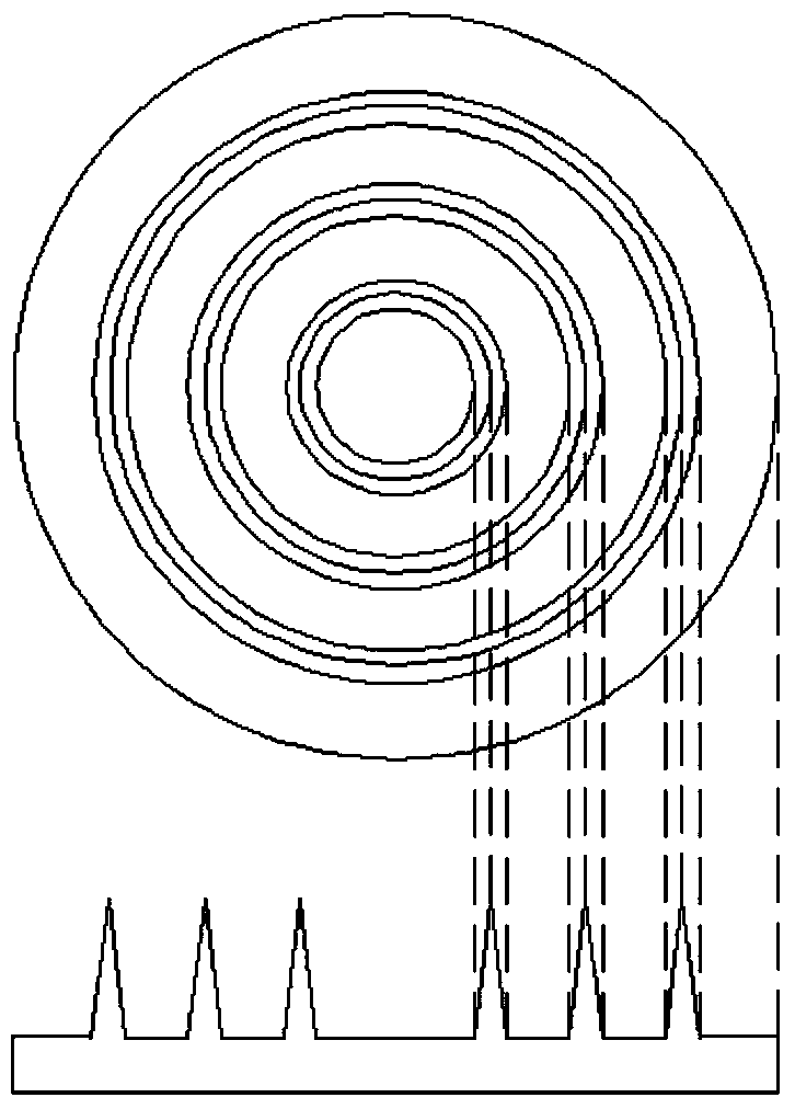
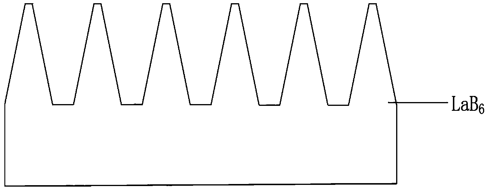
The invention belongs to the technical field of emission of cathode fields, and specifically provides a polycrystal hexaboride annular field emission cathode and a preparation method thereof. The field emission cathode is distributed as a concentric circle annular array; the cross section of the field emission cathode is structured as that pointed tapered bulges are distributed at intervals; the field emission cathode is made from rare-earth metal or polycrystal hexaboride that is prepared through alkaline-earth metal and boron and of a CaB6 type crystal structure. Compared with the traditional pointed tapered field emission cathode, the polycrystal hexaboride annular field emission cathode is of a firm structure that effectively avoids the shortcoming that a pointed tapered field emission body is not firmly contacted with a substrate; in addition, proper mask material and corresponding electrochemical etching electrolyte composition are selected, and various process parameters are adjusted, in order to prepare a large-area polycrystal hexaboride annular field emission cathode that is outstanding in electronic emission performance; the preparation method is simple and easy to be carried out; the effective field emission area is expanded; emission current of thousands and even tens of thousands amperes can be supplied, and thus the preparation efficiency is effectively raised.

Description

technical field [0001] The invention belongs to the technical field of cathode field emission, and in particular relates to a field emission cathode and a preparation method thereof, in particular to a large-area polycrystalline hexaboride field emission cathode and a preparation method thereof. Background technique [0002] Field emission cathodes have always been at the heart of the field of vacuum microelectronics. At present, there are many kinds of field emission cathode materials, and molybdenum and silicon microtip field emission arrays are more commonly used. However, these two kinds of cathodes have the disadvantages of grids, such as the molybdenum tip is evaporated on the base, so the adhesion to the base is not strong, and the characteristics of silicon determine its poor thermal stability and low emission reliability. , The emission current is limited. Secondly, carbon nanotubes are currently considered the most promising new emitters. It has excellent physica...

Claims


Application Information

Patent Timeline
Patent Type & Authority Applications(China)
IPC IPC(8): H01J1/304H01J9/02
Inventor 林祖伦郝敏王小菊祁康成曹贵川
Owner UNIV OF ELECTRONICS SCI & TECH OF CHINA
Learn More