

Graphene doping method and doped graphene
A graphene and graphene layer technology, applied in the field of doped graphene and graphene doping, can solve the problems of unsuitable application and popularization, complicated production process, relatively large energy consumption, etc., and achieve low power consumption and diverse shapes , size and position controllable effect
- Summary
- Abstract
- Description
- Claims
- Application Information
AI Technical Summary
Problems solved by technology
Method used
Image

Examples
preparation example Construction
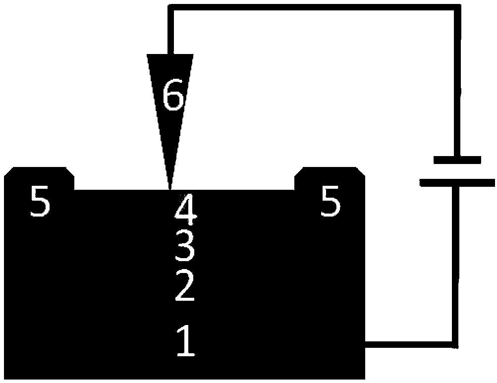
[0039] As a method for preparing a graphene device, a graphene layer can be formed on a silicon wafer having a silicon dioxide layer on the surface by the micromechanical exfoliation method described later. The silicon wafer with a silicon dioxide layer on the surface can be obtained commercially, for example, a silicon wafer commercially available from SVM Company in the United States can be used, and the thickness of the silicon wafer is 0.5 mm (for the The total thickness of the silicon wafer of the silicon dioxide layer) and has a silicon dioxide layer of 285 nm thick.
[0040] According to the present invention, by forming the polymethyl methacrylate film 4 of the present invention on the graphene layer 3, it can have the effect of storing electrostatic charges.
[0041] Preferably, the thickness of the polymethyl methacrylate film is 20-50 nm, more preferably, the thickness of the polymethyl methacrylate film is 30-45 nm, further preferably 35-45 nm.
[0042] According ...
Embodiment 1
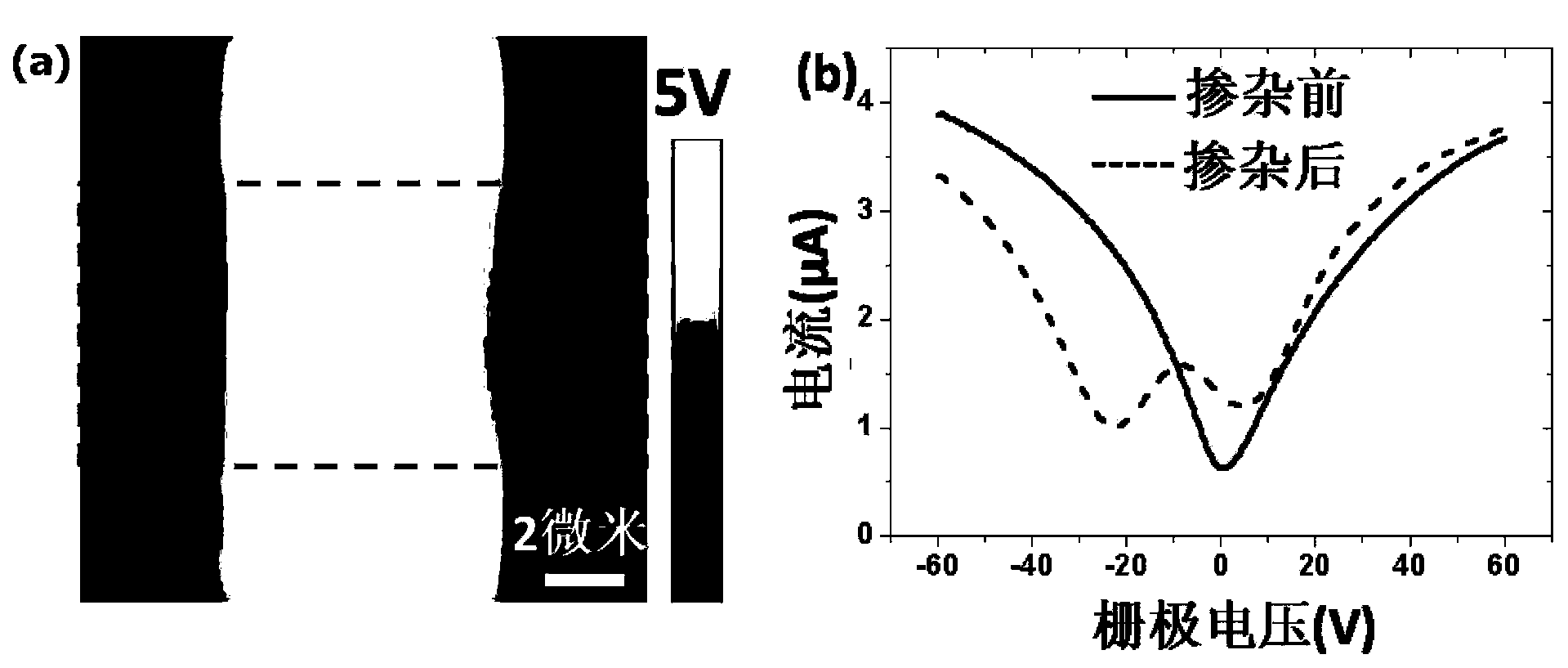
[0069] A graphene layer was fabricated on a 0.5 mm thick silicon wafer (with an oxide layer with a thickness of 285 nm on the surface) by a micromechanical exfoliation method to obtain a graphene device. A solution of polymethyl methacrylate (number-average molecular weight is 950,000, the same below) with a concentration of 4% by weight (solvent is chlorobenzene) is spin-coated on the surface of the graphene device with the graphene layer, and the spin-coating speed is 4000rpm , the spin coating time was 1.5 min, and then it was dried at 150 °C for 10 min to obtain a thin film with a thickness of 38 nm. Regions with graphene layers were found on the graphene device by atomic force microscopy (magnification mode: 1000X), and the graphene regions to be doped were precisely located by the electrostatic force microscopy mode of atomic force microscopy. Then, in the contact mode of the atomic force microscope, a voltage of 7V was applied to the conductive tip, the graphene device ...
Embodiment 2
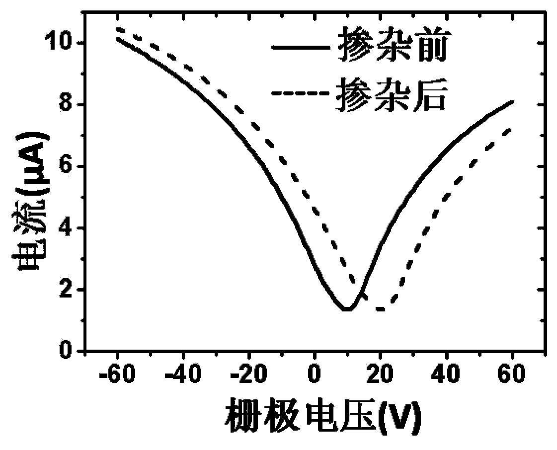
[0073] A graphene layer was fabricated on a 0.5 mm thick silicon wafer (with an oxide layer with a thickness of 285 nm on the surface) by a micromechanical exfoliation method to obtain a graphene device. The polymethyl methacrylate solution (solvent is anisole) with a concentration of 4 wt% was spin-coated on the surface of the graphene device with the graphene layer, the spin-coating speed was 4000 rpm, the spin-coating time was 2 minutes, and then After drying at 150°C for 10 minutes, a film with a thickness of 36 nm was obtained. Regions with graphene layers were found on the graphene device by atomic force microscopy (magnification mode: 1000X), and the graphene regions to be doped were precisely located by the electrostatic force microscopy mode of atomic force microscopy. Then, in the contact mode of the atomic force microscope, a voltage of 10V was applied to the conductive tip, and a voltage of -3V was applied to the silicon layer of the graphene device, and two consec...
PUM
| Property | Measurement | Unit |
|---|---|---|
| thickness | aaaaa | aaaaa |
| thickness | aaaaa | aaaaa |
| thickness | aaaaa | aaaaa |
Abstract
Description
Claims
Application Information