Master-slave follower type single-edge K value trigger constructing method utilizing circuit three-element theory and master-slave follower type single-edge K value trigger circuit

A technology with three elements of a circuit and a construction method, which is applied in the construction field of a master-slave follower type single-edge K-value flip-flop, can solve the problems such as the reduced resolution of the K-value signal of the input gate, unfavorable multi-value circuits, and reduced high-frequency performance.

Inactive Publication Date: 2015-01-21
HEILONGJIANG UNIV
View PDF7 Cites 2 Cited by
  • Summary
  • Abstract
  • Description
  • Claims
  • Application Information

AI Technical Summary

Problems solved by technology

[0002] With the rapid development of MOS integrated circuit technology, the scale of integration is getting larger and higher, and VLSI (Very Large Scale Integration) has some shortcomings: ① First, on the VLSI substrate, the wiring takes up more than 70℅ of silicon In programmable logic devices, a large number of programmable internal wiring is also required to connect each logic function block or input/output to complete a circuit with a specific function. Wiring (including programming connection switches) accounts for a large part of the material. cost
[0005] 1. In the realization of multi-valued circuits (K≥3), the existing semiconductor manufacturing process control MOS transistor threshold technology has great disadvantages: ① the range of control threshold is limited (because the ion implantation concentration is limited), and the control threshold in the process The amplitude often changes the performance of the MOS tube, and the voltage-type multi-valued circuit thus realized is not larger than the 4-valued circuit, and the application of more-valued circuits is difficult
② Only the amplitude of the threshold can be controlled, and the opening properties of the MOS tube cannot be changed (such as high-pass, low-pass, band-pass, and band-resistance). The simplest circuit structure
③ It is necessary to add an additional process of ion implantation, and the threshold can only be controlled in the semiconductor manufacturing process, which not only increases the complexity of the process, but also cannot be controlled by the user
[0006] 2. In the realization of multi-valued circuits, the existing neuron MOS transistor control threshold technology has great disadvantages: ① With the increase of K value, 'the input gate and control gate capacitance of a single neuron MOS transistor occupies the area of ​​the silicon chip' versus 'a single neuron MOS transistor'. The ratio of the MOS tube to the area of ​​the silicon chip is getting larger and larger, such as ten times, a hundred times or higher; ②As the K value increases, the width of th

Method used


Image

  • Master-slave follower type single-edge K value trigger constructing method utilizing circuit three-element theory and master-slave follower type single-edge K value trigger circuit
  • Master-slave follower type single-edge K value trigger constructing method utilizing circuit three-element theory and master-slave follower type single-edge K value trigger circuit
  • Master-slave follower type single-edge K value trigger constructing method utilizing circuit three-element theory and master-slave follower type single-edge K value trigger circuit

Examples


Embodiment 1

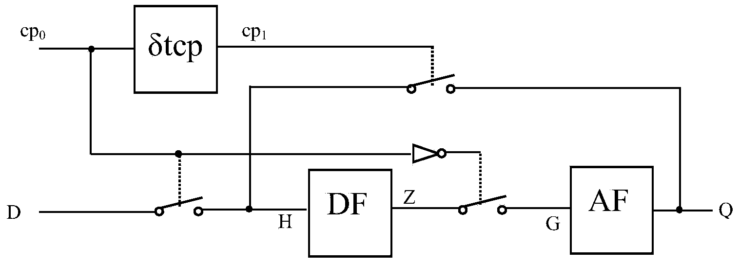
[0072] Embodiment 1: Utilize the circuit three-element theory The circuit three-element theory has formulas (5a) and (5b);

[0073] The binary value is similar to the multi-value circuit and the analog circuit. The main feature is the three elements of the circuit: signal, network and load; the multi-value signal is the rounding of the analog signal within a certain range. When the number of rounding is sufficiently large (equivalent to Since the number of scales is sufficiently large), the limit is the analog signal, and the focus of digital circuit research should be based on the "circuit behavior" of the three elements, rather than "logical realization"; it is customary to regard "logic circuit" as "logical thinking". "Logical realization", originally "circuit" and "logic" are not equivalent to each other, "circuit" is not the circuit realization of "logic", and "logic" is not the abstraction of "circuit", that is, the two are not equal If the problem is not fully descri...

Embodiment 2

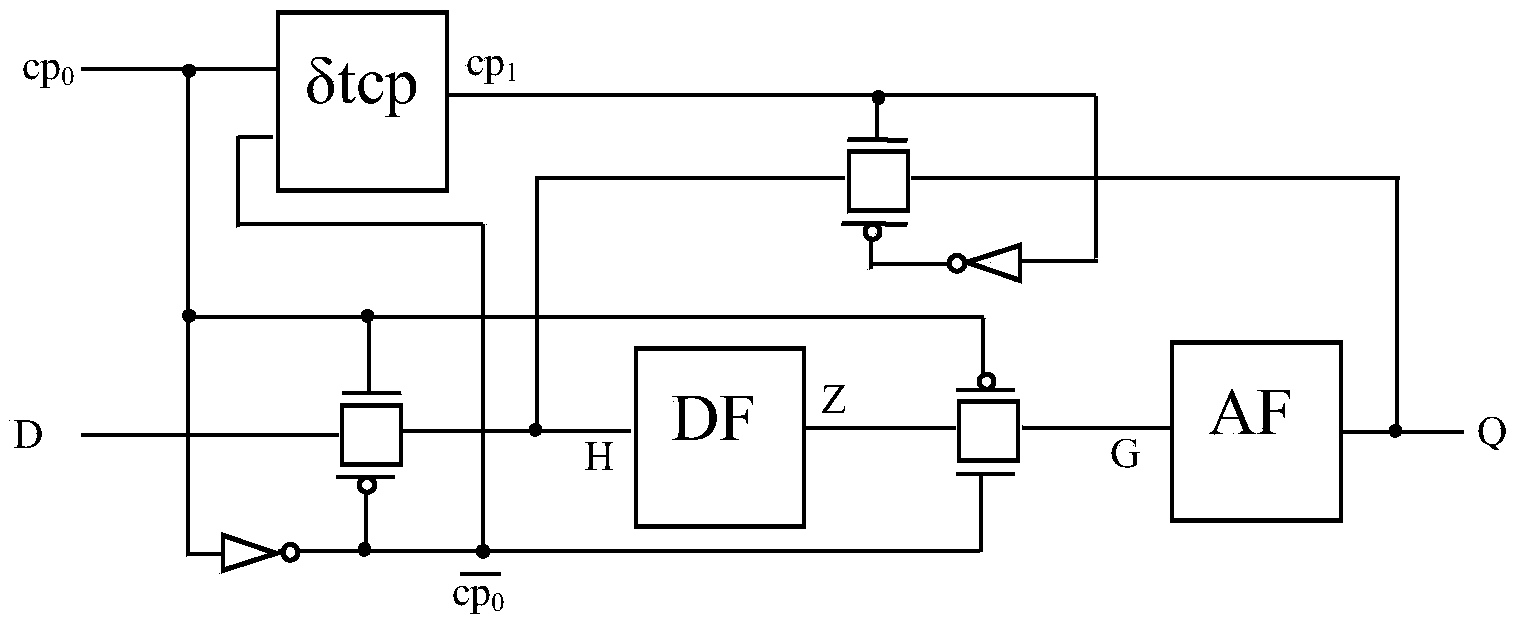
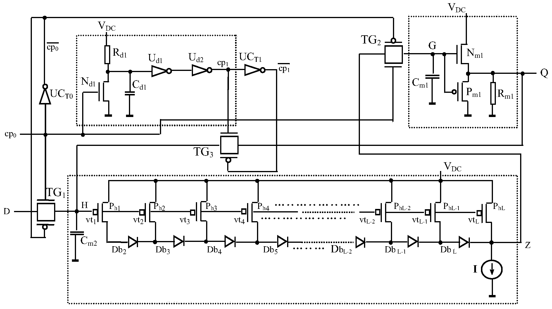
[0078] Embodiment 2: the working process of the clock falling edge delay circuit δtcp.

[0079] The clock falling edge delay circuit δtcp is shown as Figure 8 , the circuit works as follows: cp 0 Before the rising edge, the NMOS transistor N d1 cutoff, NOT gate UC d2 output cp 1 high level; when cp 0 When the rising edge comes, the tube N d1 Rapid turn-on (∵ tube N d1 gate to cp 0 ), tube N d1 Drain (i.e. Capacitance C d1 Potential and NOT gate UC d1 input) quickly drops to low level, the NOT gate UC d1 The output goes high and is sent to the NOT gate UC d2 enter, make cp 1 quickly by a high level V DC goes low, Quickly change from 0 to V DC , indicating that cp 1 falling edge (ie rising edge) and cp 0 The rising edge comes at the same time.

[0080] when cp 0 falling edge when the tube N d1 fast cut-off due to tube N d1 The drain is connected to a capacitor C d1 , so V DC Via resistor R d1 To capacitance C d1 char...

Embodiment 3

[0085] Example 3: Slave Follower AF.

[0086] The slave follower AF (analog follower) is shown as Figure 4 ,Will Figure 4 Middle PMOS tube P m1 delete, you get Figure 5 The common NMOS transistor source follower shown (by the NMOS transistor N m1 and source resistance R m1 composition), or the Figure 4 Middle source resistance R m1 delete, get Image 6 The CMOS transistor source follower shown (by the NMOS transistor N m1 and PMOS transistor P m1 composition). Because the output of the follower is connected to the gate of the next stage MOS transistor, the gate capacitance of the MOS transistor is a capacitive load to the AF output, so that Image 6 The shown CMOS transistor source follower has a hysteresis phenomenon similar to that of a Schmitt circuit. The output voltage rise and fall trajectories caused by the input voltage rise and fall are inconsistent, and the hysteresis voltage Δ=V TN +|V TP |(∵Capacitive load has a storage effect, with...


PUM

PropertyMeasurementUnit
Thicknessaaaaaaaaaa

Abstract

The invention discloses a master-slave follower type single-edge K value trigger constructing method utilizing the circuit three-element theory and a master-slave follower type single-edge K value trigger circuit. The master-slave follower type single-edge K value trigger composed of a digital follower and an analog follower is obtained by means of the circuit three-element theory, a distinctive three-beat work mode is adopted, clock falling edge triggering is adopted, an identical simplest element level circuit structure is obtained under eight optimum coding, due to the fact that a slave follower is an NMOS tube source electrode follower, only the structure scale of a main follower becomes large along with the increase of the K value which is equal to 4,5,6..., other circuit structures do not change, the main follower is the digital follower composed of a high-pass variable-threshold PMOS tube, the output logic level clamp function is realized, and the anti-jamming capability is high. The master-slave follower type single-edge K value trigger circuit is simple in structure, can serve as a K value static storage cell of a K value SSRAM, and can be used in the VLSI field such as FPGA, CPLD, semi-custom or full-custom ASIC and storer and other digital IC technical fields.

Description

(1) Technical field [0001] The invention belongs to the field of digital integrated circuits, in particular to a construction method and a circuit of a master-slave follower type single-edge K-value flip-flop using the theory of three elements of a circuit. (2) Background technology [0002] With the rapid development of MOS integrated circuit technology, the integration scale is getting larger and the integration level is getting higher and higher, and VLSI (Very Large Scale Integrated Circuit) has some deficiencies: ① First, on the VLSI substrate, the wiring occupies more than 70℅ of silicon A large number of programmable internal wirings are also required in programmable logic devices to connect various logic function blocks or input / output to complete circuits with specific functions, and wiring (including programming connection switches) occupies a large part of the material. cost. It is very important to reduce the proportion of wiring cost. ②From the perspective of ...

Claims


Application Information

Patent Timeline
IPC IPC(8): H03K3/3562
Inventor 方振贤刘莹方倩
Owner HEILONGJIANG UNIV
Why Eureka
Try Eureka