Manufacturing method of micro-nano structure capable of accurately controlling depth

A micro-nano structure and precise control technology, applied in the manufacture of micro-structure devices, micro-structure technology, micro-structure devices, etc., can solve the problems of inability to meet the high-precision requirements of micro-nano devices, affecting the diffraction effect of the device, and reducing the uniformity of the light spot. , to achieve the effect of promoting wide application, realizing mass production, reducing production cost and difficulty

Inactive Publication Date: 2015-02-04
INST OF OPTICS & ELECTRONICS - CHINESE ACAD OF SCI
View PDF4 Cites 14 Cited by
  • Summary
  • Abstract
  • Description
  • Claims
  • Application Information

AI Technical Summary

Problems solved by technology

Taking the diffractive optical device as an example, the manufacturing error of the structure, especially the longitudinal error, will seriously affect the diffraction effect of the device, resulting in a decrease in the diffraction efficiency and uniformity of the spot, which cannot meet the high precision requirements of micro-nano devices in scientific research, military industry, industry, etc. Require

Method used


Image

  • Manufacturing method of micro-nano structure capable of accurately controlling depth
  • Manufacturing method of micro-nano structure capable of accurately controlling depth
  • Manufacturing method of micro-nano structure capable of accurately controlling depth

Examples


example 1

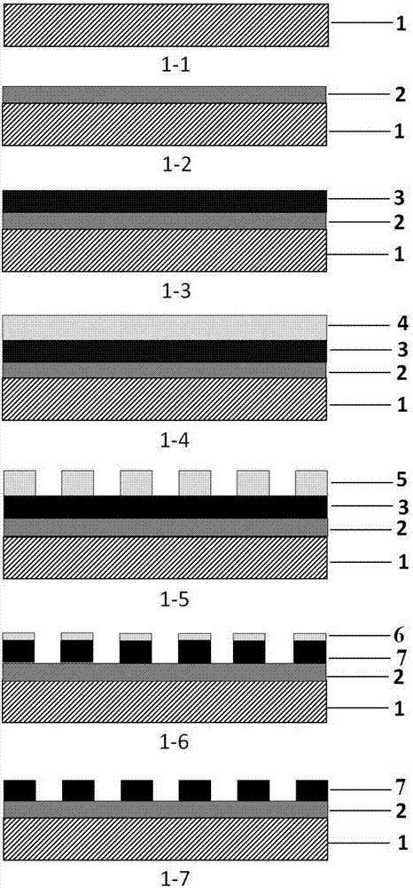
[0028] Such as figure 1 As shown in 1-1, take a polished glass substrate 1 with a thickness of 2 mm and an area of ​​3 cm x 3 cm, soak it in dilute nitric acid for more than 12 hours, remove the stain on the surface, take it out and put it in Ultrasonic cleaning in deionized water for use;

[0029] Such as figure 1 As shown in 1-2, since the gold material is resistant to reactive plasma etching of fluorine-based gases, a gold film 2 with a thickness of 305 nanometers is evaporated on the quartz substrate 1 by electron gun evaporation as an etching cut-off. layer;

[0030] Such as figure 1 As shown in 1-3, a silicon dioxide film 3 with a thickness of 900 nanometers is coated on the gold film 2 by magnetron sputtering, and the thickness of the film layer is detected online by an online quartz crystal film thickness measuring instrument. Accuracy is ±1 nanometer;

[0031] Such as figure 1 As shown in middle 1-4, use the glue leveler, set the rotation speed to 3000 rpm, spin...

example 2

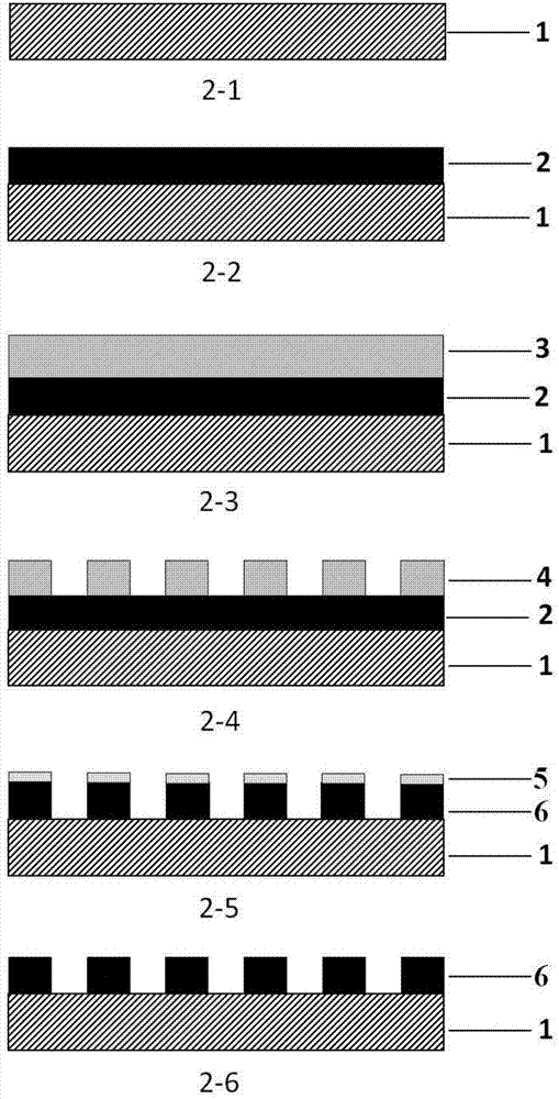
[0035] Such as figure 2 As shown in 2-1, take an aluminum oxide substrate with a surface polishing thickness of 2 mm and an area of ​​3 cm × 3 cm as the etching stop layer 1, and clean the surface with acetone solution to remove the surface stains;

[0036] Such as figure 2 As shown in middle 2-2, a layer of silicon nitride material film 2 with a thickness of 1.8 microns is coated on the aluminum oxide substrate 1 by magnetron sputtering, and the thickness of the film layer is measured by an online quartz crystal film thickness measuring instrument. On-line detection, the thickness accuracy is ±1 nanometer;

[0037] Such as figure 2 As shown in middle 2-3, use a glue homogenizer, set the speed at 5000 rpm, spin-coat the photoresist AZ9260 on the surface of the silicon nitride film 2 to form a photoresist film layer 3 with a thickness of 2.537 microns, The accuracy of spin coating is ±3 nanometers;

[0038] Such as figure 2 As shown in 2-4, a photoresist grating struc...


PUM

PropertyMeasurementUnit
depthaaaaaaaaaa
depthaaaaaaaaaa
thicknessaaaaaaaaaa

Abstract

The invention relates to a manufacturing method of a micro-nano structure capable of accurately controlling depth, which belongs to the technical field of processing of advanced materials and micro-nano structures. The manufacturing method comprises the following steps: selecting an etching resistant material to form an etching cutoff layer, and forming a structural material layer with the thickness being target depth on the surface of the etching cutoff layer by utilizing a film technique; then coating the surface of the structural layer with a layer of etching resistant agent, and manufacturing the required micro-nano structure on the etching resistant agent by utilizing a micro-nano processing technique; with the micro-nano structure on the etching resistant agent as a mask, transferring the micro-nano structure onto the structural material layer by utilizing an etching transferring process until the micro-nano structure reaches the etching cutoff layer with etching resistance, and stopping etching; and removing the etching resistant agent which remains on the structural layer so as to obtain the micro-nano structure of which the depth is up to a target value, wherein the depth precision is increased to + / -5 nanometers. The manufacturing method has the advantages of low cost, large local processing figure area, high precision and good uniformity, and wide application of high-precision optical devices to scientific research and production is promoted.

Description

technical field [0001] The invention belongs to the technical field of micro-nano structure processing, and relates to a method for manufacturing a micro-nano structure with precisely controlled depth. Background technique [0002] With the development of advanced micro-nano processing technology, micro-nano structures have more and more applications in optics, electronics, biochemistry, etc. Improving the manufacturing precision of micro-nanostructures and reducing structural errors (lateral and longitudinal errors) are the key factors to promote its application. Taking the diffractive optical device as an example, the manufacturing error of the structure, especially the longitudinal error, will seriously affect the diffraction effect of the device, resulting in a decrease in the diffraction efficiency and uniformity of the spot, which cannot meet the high precision requirements of micro-nano devices in scientific research, military industry, industry, etc. Require. There...

Claims


Application Information

Patent Timeline
Patent Type & Authority Applications(China)
IPC IPC(8): B81C1/00B82Y40/00
Inventor 邓启凌张满秦燕云史立芳曹阿秀庞辉
Owner INST OF OPTICS & ELECTRONICS - CHINESE ACAD OF SCI
Why Eureka
Try Eureka