Method for manufacturing fast-recovery glass package diode with ultra-high voltage above 13,000 V

A technology of glass encapsulation and manufacturing method, which is applied in semiconductor/solid-state device manufacturing, electrical components, electric solid-state devices, etc. It can solve the problems of large forward power loss, unsuitability for mass production, and large volume of silicon stacks, etc., and achieve reduction Encapsulation volume, high long-term working reliability, and small size effect

Active Publication Date: 2015-02-25
西安卫光科技有限公司
View PDF7 Cites 4 Cited by
  • Summary
  • Abstract
  • Description
  • Claims
  • Application Information

AI Technical Summary

Problems solved by technology

However, due to the series connection of multiple diodes, the process is complicated and not suitable for mass production. The silicon stack after series connection is bulky and inconvenient to install. The total forward voltage drop of the silicon stack after series connection is the sum of the bulk voltage drop of each diode. Large forward power loss and poor rectification effect during operation

Method used


Image

  • Method for manufacturing fast-recovery glass package diode with ultra-high voltage above 13,000 V
  • Method for manufacturing fast-recovery glass package diode with ultra-high voltage above 13,000 V
  • Method for manufacturing fast-recovery glass package diode with ultra-high voltage above 13,000 V

Examples


Embodiment Construction

[0047] In order to make the object, technical solution and advantages of the present invention clearer, the implementation manner of the present invention will be further described in detail below in conjunction with the accompanying drawings.

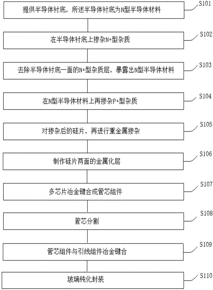
[0048] combine figure 1 The flow chart of the present invention illustrates the method step of the present invention:

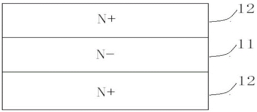
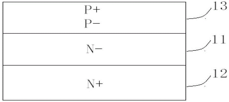
[0049] Step S101, providing a semiconductor substrate, the semiconductor substrate is an N-type semiconductor silicon material, and different material resistivities can be selected according to different reverse voltages. In order to ensure a reverse voltage above 13,000 volts, the voltage of a single tube must be at least Above 1500V, the resistivity of the material should be selected at 40-50Ω.cm, and the thickness of the N-type substrate should be 500μm; see figure 2 N-type silicon material layer 11;

[0050] Step S102, doping N on the N-type semiconductor substrate + Type impurities (phosphorous oxides, such a...


PUM


Abstract

The invention discloses a method for manufacturing a fast-recovery glass package diode with an ultra-high voltage above 13,000 V. The method comprises the steps that N type semiconductor silicon materials are adopted as a semiconductor substrate, N+ type impurities are doped on the N type semiconductor substrate, an N+ type impurity layer on one face of the semiconductor substrate is removed, P+ type impurities are dually doped on exposed N- type semiconductor materials, then heavy metal platinum doping is carried out, metallization layers on the two faces of a silicon wafer are manufactured through a vacuum coating technology, a plurality of chips are bonded to a pipe core assembly in a metallurgy mode, the silicon wafer is divided into pipe cores of the needed size, the divided pipe core assembly and a lead assembly are bonded through high-temperature sintering and metallurgy, glass passivation and packaging are carried out, adjusted glass powder paste coats the twelve pipe cores connected in series, and manufacturing of the glass package diode is completed. The method has the advantages of being high in voltage, small in forward direction, fast in reverse restoration, good in high-temperature work stability, high in long-term work stability and the like, and is widely applied to the field of aviation, aerospace, electronics, weapons, ships and the like.

Description

technical field [0001] The invention belongs to the technical field of semiconductors, and relates to a method for manufacturing an ultra-high voltage and fast-recovery glass-encapsulated diode of more than 13,000 volts. Background technique [0002] In large-scale or high-voltage circuits, due to the low reverse withstand voltage of general rectifier diodes, the PN junction is broken down in the negative half cycle and cannot complete the rectification function. Therefore, silicon stacks are generally composed of multiple diodes in series at home and abroad. Achieve high reverse withstand voltage. However, due to the series connection of multiple diodes, the process is complicated and not suitable for mass production. The silicon stack after series connection is bulky and inconvenient to install. The total forward voltage drop of the silicon stack after series connection is the sum of the bulk voltage drop of each diode. When working, the forward power loss is large, and t...

Claims


Application Information

Patent Timeline
Patent Type & Authority Applications(China)
IPC IPC(8): H01L21/329
CPCH01L21/2855H01L21/56H01L25/50H01L29/66136
Inventor 王嘉蓉
Owner 西安卫光科技有限公司
Why Eureka
Try Eureka