

Non-selective wet etching solution for III-V semiconductor materials as well as preparation method and application of non-selective wet etching solution
A non-selective, wet etching technology, applied in the direction of chemical instruments and methods, surface etching compositions, etc., can solve the problems of affecting electrical parameters, uneven corrosion profiles, unsuitable for industrial production, etc., and achieve material cost The effect of low cost and simple process
- Summary
- Abstract
- Description
- Claims
- Application Information
AI Technical Summary
Problems solved by technology
Method used
Image

Examples
Embodiment 1
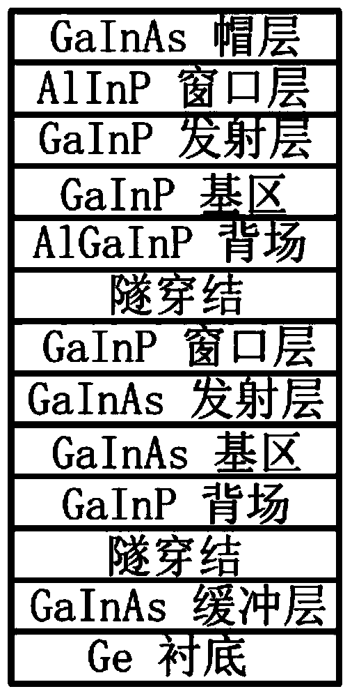
[0030] The non-selective wet etching solution for III-V semiconductor materials of the present invention has the following components by weight percentage: 4%-8% potassium dichromate, 18%-51% concentrated hydrochloric acid, 36%-66% phosphoric acid , 8%-9% deionized water, through this corrosive solution can realize the non-toxicity of multi-component compound materials represented by GaAs system, InP system, III-V group, such as single substance, binary, ternary, quaternary, etc. Selective wet etching can also realize non-selective wet etching of metal materials such as Ge substrates, Au / Ag / AuGeNi, etc. The etching formula is not affected by the concentration of epitaxial dopant. A typical triple-junction GaAs solar cell structure such as figure 1 shown.
[0031] Below we take single-junction and triple-junction GaAs solar cells as corrosion objects, and describe the present invention in detail, and the details are as follows:
[0032] 1. Preliminary preparation for corrosio...
Embodiment 2
[0051] Also take single-junction and triple-junction GaAs solar cells as the corrosion objects, and the specific conditions are as follows:
[0052] 1. Preliminary preparation for corrosion
[0053] 1.1) Use acetone and HCl solution to remove organic and inorganic contamination on the surface of single-junction and triple-junction GaAs solar cell epitaxial wafers;
[0054] 1.2) The above-mentioned epitaxial wafers are flushed with water in the quick-discharging rinsing tank to remove cleaning residues until the water resistance reaches above 10MΩ;
[0055] 1.3) Dry the rinsed epitaxial wafer in a dryer to remove residual water stains;
[0056] 1.4) The cleaned epitaxial wafer is sequentially subjected to processes such as yellow light uniform coating, photolithography, development, and baking, and photoresist is used to form a mesa pattern on the surface of the epitaxial layer to be etched;
[0057] 1.5) Coating a layer of photoresist on the back of the above-mentioned epitaxi...
PUM
 Abstract
Description
Claims
Application Information