Sand-blasting-free diffusion nickel plating technology of rectification monocrystalline silicon wafer

A monocrystalline silicon wafer and process technology, applied in the direction of electrical components, semiconductor/solid-state device manufacturing, circuits, etc., can solve the problems of polluted environment, excessive dust, vibration and noise, etc., to reduce production costs, low production costs, The effect of high product quality

Inactive Publication Date: 2015-03-04
程德明
View PDF8 Cites 7 Cited by
  • Summary
  • Abstract
  • Description
  • Claims
  • Application Information

AI Technical Summary

Problems solved by technology

[0005] In addition to the huge energy consumption and the fragments and stress caused by the mechanical impact of the monocrystalline silicon wafer, the vibration and noise of the air compressor after starting are huge, and are affected by it within a distance of 1 kilometer; the sand and dust ejected by the san

Method used


Image

  • Sand-blasting-free diffusion nickel plating technology of rectification monocrystalline silicon wafer
  • Sand-blasting-free diffusion nickel plating technology of rectification monocrystalline silicon wafer

Examples


Embodiment Construction

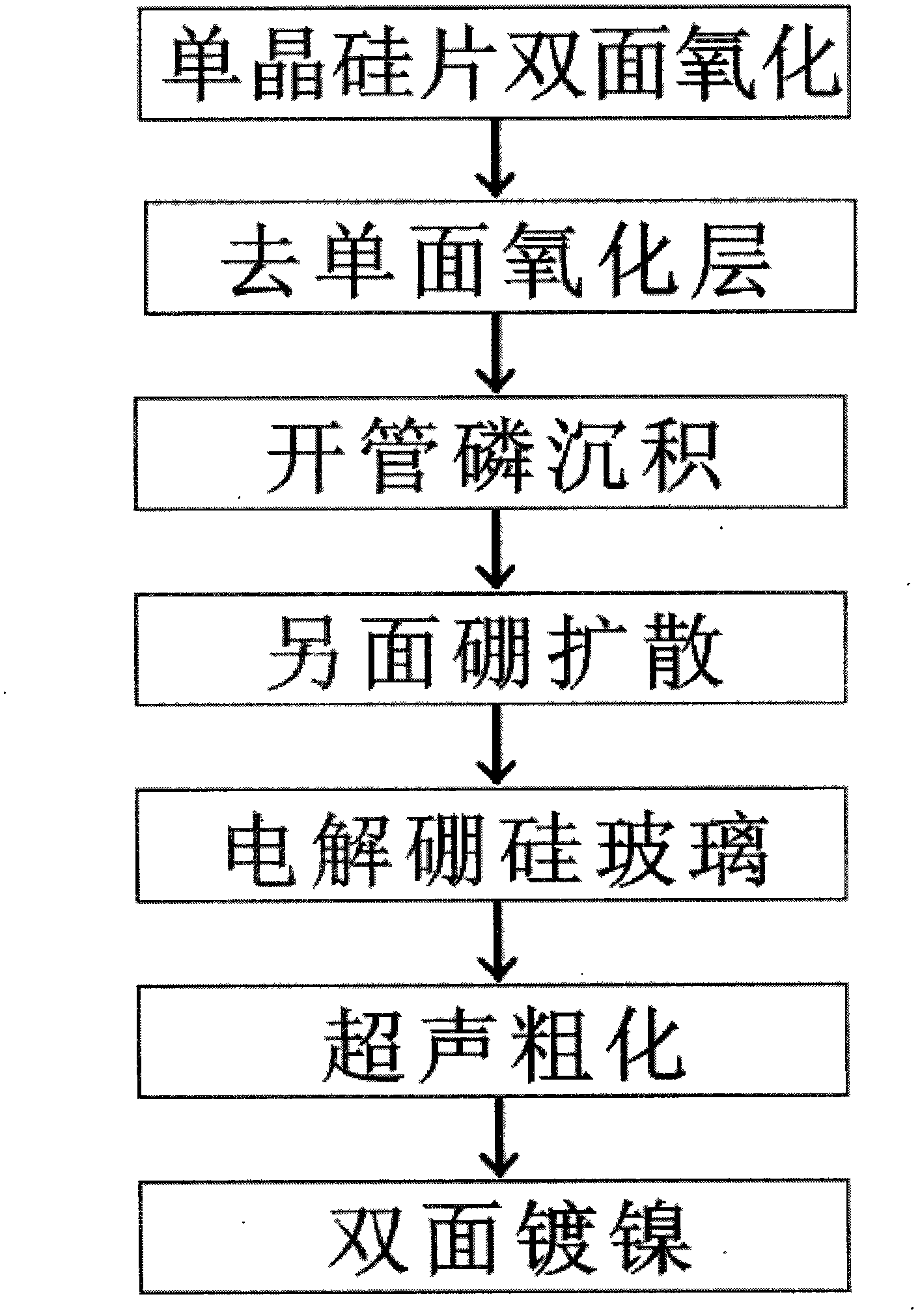
[0024] The main process flow of the rectifying single crystal silicon wafer free of sandblasting diffusion nickel plating process of the present invention is: double-sided grinding of N-type single crystal silicon wafer (raw material) - double-sided oxidation - removal of single-sided oxide layer - open-tube phosphorus deposition - Boron diffusion on the other side - Electrolytic borosilicate glass - Ultrasonic roughening - Nickel plating on both sides - Rectifying single crystal silicon wafer (product). The block diagram of its technological process is shown in the appendix of the manual. figure 2 . This manual only focuses on the implementation of new processes that have been added or transformed, and the processes that still need to be retained in traditional processes are not introduced.

[0025] The implementation of the "double-sided oxidation process": double-sided grinding of single-crystal silicon wafers, after cleaning, the double-sided oxidation process is carried...


PUM


Abstract

Provided in the invention is a sand-blasting-free diffusion nickel plating technology of a rectification monocrystalline silicon wafer. According to the invention, the oxidation technology, the electrolysis technology, and the ultra sand coarsening technology technology are used for replacing the traditional sand blasting technology. The provided technology has advantages of energy conservation and power consumption reduction, good noise-free and dust-free properties, low production cost, and high product quality and the like and thus is the preferred one for technical transformation of the ectification monocrystalline silicon wafer diffusion nickel plating enterprise.

Description

technical field [0001] The sandblasting-free diffusion nickel plating process technology for rectifying single crystal silicon wafers belongs to the "Catalogue of High-tech Fields Key Supported by the State", the key technology field of green manufacturing and pollution reduction in the electronics industry. Background technique [0002] Rectifier diodes and bridge rectifiers are the basic components of the electronics industry, and the annual demand in the Chinese market is tens of billions. The raw material for manufacturing this kind of product is single crystal silicon wafer. A PN junction is formed in the single crystal silicon wafer by diffusion process. The silicon wafer is cut into the required area and shape, and then processed in the subsequent process. It is possible to manufacture rectifier components of various specifications. [0003] At present, the main process flow of the rectifying single crystal silicon wafer manufacturing process in China is as follows:...

Claims


Application Information

Patent Timeline
IPC IPC(8): H01L21/02
CPCH01L21/0201H01L21/02013H01L21/02697
Inventor 程德明程学飞王玲珍程云飞
Owner 程德明
Why Eureka
Try Eureka