Detection method for tellurium zinc cadmium wafer damage layer thickness
The technology of a cadmium zinc telluride wafer and a detection method, which are applied to measurement devices, instruments, optical devices, etc., can solve the problems of long time consumption, different corrosive liquid systems, unsuitable for rapid routine detection, etc., and achieve intuitive, accurate and practical results. high effect
- Summary
- Abstract
- Description
- Claims
- Application Information
AI Technical Summary
Problems solved by technology
Method used
Image

Examples
Embodiment 1
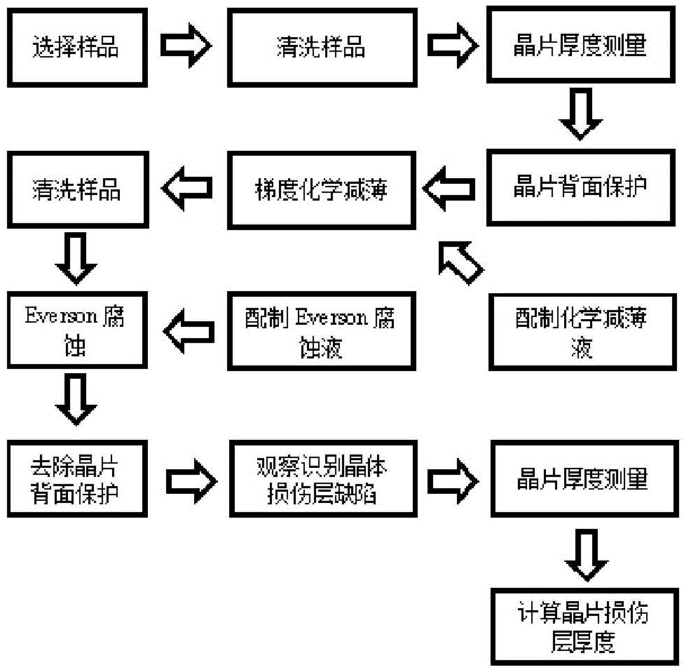
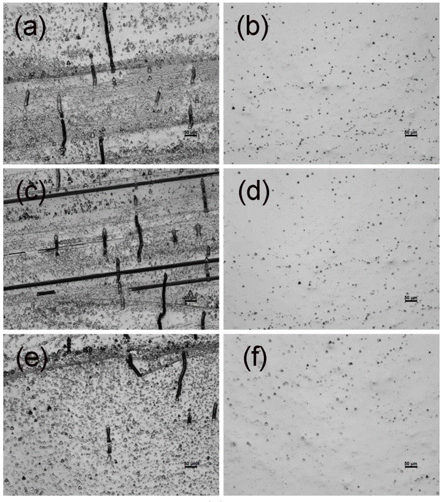
[0027] 1 Take the cadmium zinc telluride wafer processed along the (111) plane, with a single crystal area of 10mm X 20mm.
[0028] 2 Clean the cadmium zinc telluride wafer with boiling absolute ethanol, then clean it with boiling isopropanol, take it out and dry it for later use.
[0029] 3 Use the Z-axis microscope to measure the original thickness of the wafer center point and record it as t 0 (um).
[0030] 4Protect the (111)A surface of the wafer with a mucous film, and the size of the film should fit the size of the single wafer as much as possible.
[0031] 5 Preparation of chemical thinning solution: liquid bromine with a mass concentration of 99.5%: methanol with a mass concentration of 99.7% by volume ratio is 1:99 to prepare a chemical thinning solution, at this time the volume fraction of 1% bromine methanol solution is obtained , Stir well and set aside.
[0032] 6 Prepare a transparent quartz beaker, put the sample to be tested into the beaker vertically, use the droppi...
Embodiment 2
[0041] 1 Take the cadmium zinc telluride wafer processed along the (111) plane, with a single crystal area of 20mm X 30mm.
[0042] 2 Clean the cadmium zinc telluride wafer with boiling absolute ethanol, then clean it with boiling isopropanol, take it out and dry it for later use.
[0043] 3 Use a Z-axis microscope to measure the original thickness of the center point of the wafer and record it as t0 (um).
[0044] 4Protect the (111)A surface of the wafer with a mucous film, and the size of the film is as close as possible to the size of the single wafer.
[0045] 5 Preparation of chemical thinning solution: liquid bromine with a mass concentration of 99.5%: methanol with a mass concentration of 99.7% by volume ratio is 3:97 to prepare a chemical thinning solution. At this time, a 3% bromine methanol solution is obtained , Stir well and set aside.
[0046] 6 Prepare a transparent quartz beaker, put the sample to be tested into the beaker vertically, use the dropping funnel to slowly ...
Embodiment 3
[0055] 1 Take the cadmium zinc telluride wafer processed along the (111) plane, with a single crystal area of 30mm X 40mm.
[0056] 2 Clean the cadmium zinc telluride wafer with boiling absolute ethanol, then clean it with boiling isopropanol, take it out and dry it for later use.
[0057] 3 Use the Z-axis microscope to measure the original thickness of the wafer center point and record it as t 0 (um).
[0058] 4Protect the (111)A surface of the wafer with a mucous film, and the size of the film is as close as possible to the size of the single wafer.
[0059] 5 Preparation of chemical thinning solution: liquid bromine with a mass concentration of 99.5%: methanol with a mass concentration of 99.7% by volume ratio is 5:95 to prepare a chemical thinning solution, and the volume fraction of bromine methanol solution with 5% is obtained at this time , Stir well and set aside.
[0060] 6 Prepare a transparent quartz beaker, put the sample to be tested into the beaker vertically, use the d...
PUM
 Abstract
Description
Claims
Application Information
 - R&D
- Intellectual Property
- Life Sciences
- Materials
- Tech Scout
- Unparalleled Data Quality
- Higher Quality Content
- 60% Fewer Hallucinations
Browse by: Latest US Patents, China's latest patents, Technical Efficacy Thesaurus, Application Domain, Technology Topic, Popular Technical Reports.
© 2025 PatSnap. All rights reserved.Legal|Privacy policy|Modern Slavery Act Transparency Statement|Sitemap|About US| Contact US: help@patsnap.com