

Super capacitor based on three-dimensional ZnO@MnO2 composite nano array interdigital electrode and manufacturing method thereof
A technology of supercapacitors and interdigitated electrodes, which is applied in the field of energy storage, can solve the problems that it is difficult to adapt to the development requirements of high-power and high-energy flexible transparent supercapacitors, it is difficult to apply solid-state electronic devices, and the capacitors are low, so as to meet the requirements of high-power , meet the charging and discharging needs, long life effect
- Summary
- Abstract
- Description
- Claims
- Application Information
AI Technical Summary
Problems solved by technology
Method used
Image

Examples
Embodiment 1
[0045] Preparation of ZnOMnO 2 Composite nanoarray interdigitated electrodes
[0046] 1. Substrate selection: choose PET as the substrate, and treat it with an oxygen plasma surface treatment machine for 2 minutes.
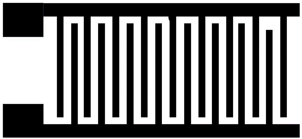
[0047] 2. Design of interdigitated electrodes: use semiconductor device micro-processing technology to process interdigitated electrode patterns on PET substrates. The pattern design of the interdigitated electrode used as a UV lithography mask is as follows: figure 1 shown. It can be seen from the figure that the number of pairs of prepared interdigital electrodes is 8 pairs, and the spacing and finger width between the interdigital electrodes are 100 microns. The operating conditions of the photolithography process are: the photoresist model used for ultraviolet lithography is AZ4620, the coating thickness is 3 microns, the coating speed is 2000 rpm, the pre-baking temperature is 105 degrees, the exposure time is 25s, and the developing time For 70s, an inte...
Embodiment 2
[0053] Fabrication of flexible transparent solid-state 3D supercapacitors
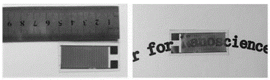
[0054] Dissolve lithium chloride and PVA in an appropriate amount of deionized water at a mass ratio of 2:1, and stir in a water bath at 85°C for 1 hour to obtain a solid electrolyte. Spread the solid electrolyte evenly on the prepared interdigitated capacitor and encapsulate it with PMMA to obtain a flexible transparent solid supercapacitor, such as Figure 4 As shown, it can be seen from the figure that the solid supercapacitor has a length of about 5 cm, high transparency, can be bent, and has good flexibility. The cyclic voltammetry curves of the prepared flexible transparent solid supercapacitor are as follows: Figure 5 As shown, it can be seen from the figure that at different scan rates, the CV curves have a nearly rectangular structure, which is a typical amorphous MnO 2 Capacitive characteristics, at a scan rate of 2mV / s, the area capacitance of the device can reach 167mF / cm -2 . Figure ...
Embodiment 3
[0056] Preparation of ZnOMnO 2 Composite Nanoarray Interdigitated Electrodes
[0057] 1. Substrate selection: select PDMS as the substrate, and treat it with an oxygen plasma surface treatment machine for 2 minutes.
[0058] 2. Design of interdigitated electrodes: use semiconductor device micromachining technology to process interdigitated electrode patterns on PDMS substrates. The pitch and finger width of the interdigitated electrodes used as a UV lithography mask are 2 μm. The operating conditions of the photolithography process are: the photoresist model used for ultraviolet lithography is AZ4620, the coating thickness is 4 microns, the coating speed is 1000 rpm, the pre-baking temperature is 80 degrees, the exposure time is 15s, and the developing time For 65s, an interdigitated electrode pattern was prepared on the PDMS substrate.
[0059] 3. Preparation of collector electrode and ZnO seed layer: a 60nm Pt thin film and a 10nm ZnO thin film were deposited on the PDMS ...
PUM
| Property | Measurement | Unit |
|---|---|---|
| Thickness | aaaaa | aaaaa |
| Thickness | aaaaa | aaaaa |
| Thickness | aaaaa | aaaaa |
Abstract
Description
Claims
Application Information