
Manufacturing method for nitride light emitting diode

A technology of light-emitting diodes and nitrides, applied in semiconductor devices, electrical components, circuits, etc., can solve the problems of limited voltage and other electrical properties, affecting growth yield, and disadvantages, and achieves improved electrical uniformity and light extraction efficiency. , The effect of improving the voltage and electrical properties

Active Publication Date: 2015-04-08
ANHUI SANAN OPTOELECTRONICS CO LTD
View PDF3 Cites 1 Cited by
  • Summary
  • Abstract
  • Description
  • Claims
  • Application Information

AI Technical Summary

Problems solved by technology

[0004] However, when the conventional metal-organic chemical vapor deposition method (MOCVD method) is used to epitaxially grow LED materials on the surface of the patterned substrate, the depth of the pattern on the surface of the patterned substrate is required to be less than 2 microns. When the depth value is greater than this value, The MOCVD method cannot obtain a good-quality epitaxial film layer; in addition, due to the uneven surface characteristics of the patterned substrate, it is necessary to laminate a thicker buffer layer between the n-type layer and the substrate in the LED structure to make the n-type layer grow. The surface of the previous epitaxial layer reaches the required smooth structure, which is beneficial to the lamination of the subsequent epitaxial layer. However, the thicker underlying structure produces greater stress, which causes the warped LED structure to be larger, which is not conducive to the implementation of subsequent processes (such as subsequent cracks in the manufacturing process), and cause significant differences in the electrical properties of each part of the monolithic LED structure, affecting the growth yield; and due to the quality of the bottom layer, the doping concentration of the active layer is also limited by it, and a higher doping level cannot be obtained , thus limiting the further improvement of the voltage equielectricity

Method used


Image

  • Manufacturing method for nitride light emitting diode
  • Manufacturing method for nitride light emitting diode
  • Manufacturing method for nitride light emitting diode

Examples


Embodiment 1

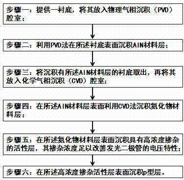
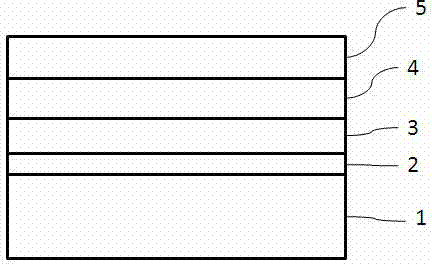
[0036] Please see attached figure 1 and 2 , providing a substrate 1, which is a flat substrate or a patterned substrate, and its material is sapphire, silicon, silicon carbide, gallium nitride or gallium arsenide, etc., wherein the vertical height range of the graphics in the patterned substrate is 2 ~20 microns, the pattern can be formed by dry etching or wet etching; put this large-depth substrate 1 into a PVD chamber, adjust the temperature of the chamber to 350-550°C, and the pressure to 2-10mtorr, using PVD The method deposits an AlN material layer 2 with a flat surface and a thickness of 5 to 350 angstroms on the surface of the substrate 1; due to the film-forming characteristics of the PVD method, when the pattern depth of the patterned substrate is higher than the depth of the conventional substrate, the AlN material layer 2 can still maintain the characteristics of smooth surface and good film quality; then take out the substrate deposited with AlN material layer 2, ...

Embodiment 2

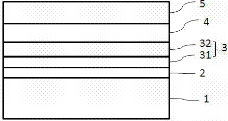
[0038] Please see attached image 3, providing a substrate 1, which is a flat substrate or a patterned substrate, and its material can be sapphire, silicon, silicon carbide, gallium nitride or gallium arsenide, etc.; when a patterned substrate is selected, the vertical height of the pattern The range is 2-20 microns, and its pattern is formed by dry etching or wet etching; put this large-depth substrate 1 into a PVD chamber, adjust the chamber temperature to 350-550°C, and the pressure to 2-10mtorr. The method deposits an AlN material layer 2 with a flat surface and a thickness of 5 to 350 angstroms on the surface of the substrate 1; due to the film-forming characteristics of the PVD method, when the pattern depth of the substrate used is higher than that of a conventional patterned substrate, the AlN material layer 2 can still maintain the characteristics of smooth surface and good film quality; then take out the substrate deposited with AlN material layer 2, put it into the ...

Embodiment 3

[0040] Please see attached Figure 4 , this embodiment is optimized on the basis of Embodiment 2, that is, when the substrate deposited with the AlN material layer 2 is taken out and put into the chemical vapor deposition (CVD) chamber, the temperature of the chamber is adjusted to 200 -900°C, on the surface of the AlN material layer 2, first deposit a low-temperature gallium nitride layer 30 with a thickness of 5 angstroms to 1500 angstroms, and then raise the chamber temperature to above 900°C to deposit a high-temperature non-doped gallium nitride layer 31, Then deposit the n-type gallium nitride layer 32 , and finally adjust the temperature of the chamber to continue depositing the doped active layer 4 and the p-type layer 5 .

[0041] In this embodiment, the low-temperature gallium nitride layer 30 is first deposited on the AlN material layer, and then the low-temperature gallium nitride layer 30 is subjected to an elevated temperature annealing treatment before the high-...


PUM

PropertyMeasurementUnit
heightaaaaaaaaaa
temperatureaaaaaaaaaa
thicknessaaaaaaaaaa

Abstract

The invention provides a manufacturing method for a nitride light emitting diode. The method comprises: using a PVD method to deposit an AIN film layer on a patterned substrate with larger depth, using a CVD method to deposit a nitride epitaxial layer on the AIN film layer, the thickness of the nitride epitaxial layer being relatively thin, through reducing the little stress of the epitaxial layer, improving warping of an epitaxial wafer, so as to improve electrical property uniformity of a single epitaxial wafer; using the patterned substrate with larger depth to improve light extraction efficiency; and mixing high density impurity in an active layer, under the condition of not influencing leakage, the impurity effectively reducing voltage feature, so as to improve integrated yield of the light emitting diode.

Description

technical field [0001] The invention relates to a method for preparing a light-emitting diode, which belongs to the technical field of light-emitting diode manufacture. Background technique [0002] Physical vapor deposition (Physical Vapor Deposition, PVD) technology refers to the use of physical methods under vacuum conditions to vaporize the material source—solid or liquid surface into gaseous atoms, molecules or parts of ionization into ions, and through low-pressure gas (or plasma) Body) process, the technology of depositing a thin film with a certain special function on the surface of the substrate. Physical vapor deposition methods mainly include: vacuum evaporation, sputtering coating, arc plasma plating, ion coating, and molecular beam epitaxy, etc.; it can not only deposit metal films, alloy films, but also deposit compounds, ceramics, semiconductors, polymers, etc. Membranes, etc.; this technology has a simple process, less environmental pollution, less consumpti...

Claims


Application Information

Patent Timeline
Patent Type & Authority Applications(China)
IPC IPC(8): H01L33/00
CPCH01L33/00H01L33/0075
Inventor 谢翔麟李政鸿徐志波林兓兓卓昌正张家宏
Owner ANHUI SANAN OPTOELECTRONICS CO LTD
Learn More