Encapsulation structure and encapsulation method of organic light emitting diode device
An electroluminescent device and packaging structure technology, applied in the direction of electro-solid devices, electrical components, semiconductor devices, etc., can solve the problems of loss of desiccant absorption capacity, decreased device life, easy to generate cracks, etc., to achieve good step coverage and The effect of large area thickness uniformity, small influence and strong adhesion
- Summary
- Abstract
- Description
- Claims
- Application Information
AI Technical Summary
Problems solved by technology
Method used
Image
Examples
Embodiment 1
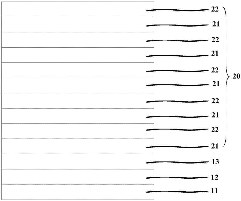
[0058] figure 1 It is a schematic diagram of the packaging structure of the organic electroluminescent device in Example 1; as figure 1 As shown, the packaging structure of the organic electroluminescent device includes an ITO glass substrate 11, an organic light-emitting functional layer 12, a cathode 13, and a thin film encapsulation layer 20; the thin film encapsulation layer 20 includes five germanium carbide film layers 21 and an inorganic barrier layer 22 package units.
[0059] A method for encapsulating an organic electroluminescent device, comprising the steps of:
[0060] (1) Pre-treatment of ITO glass substrate (11): First, clean the ITO glass with acetone, ethanol, deionized water, and ethanol in sequence, all of which are cleaned with an ultrasonic cleaner. dry, oven dry stand-by; then carry out surface activation treatment to the cleaned ITO glass, to increase the oxygen content of the conductive surface layer, improve the work function of the conductive layer ...
Embodiment 2
[0076] A method for encapsulating an organic electroluminescent device, comprising the steps of:
[0077] (1), (2), (3) are the same as embodiment 1;
[0078] (4) Preparation of thin film encapsulation layer:
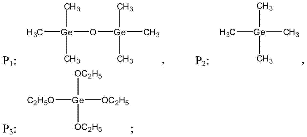
[0079] a) Preparation of germanium oxycarbide film layer: Plasma-enhanced chemical vapor deposition (PECVD) was used to prepare a germanium oxycarbide film layer on the cathode surface, the working pressure was 80Pa, the deposition temperature was 60°C, and the radio frequency power was 1W / cm 2 ; The gas source adopted in the process of depositing germanium oxycarbide layer is tetramethylgermane (TMG) and dinitrogen monoxide (N 2 O), the loading gas is argon (Ar); the flow of tetramethylgermane (TMG) is 25sccm, nitrous oxide (N 2 O), the flow of argon (Ar) mixed gas is 50sccm, nitrous oxide (N 2 O) and nitrous oxide (N 2 O), the ratio R of argon (Ar) mixed gas flow is 60%; The thickness of germanium oxycarbide film layer is 280nm;
[0080] b) Preparation of inorgan...
Embodiment 3
[0085] A method for encapsulating an organic electroluminescent device, comprising the steps of:
[0086] (1), (2), (3) are the same as embodiment 1;
[0087] (4) Preparation of thin film encapsulation layer:
[0088] a) Preparation of germanium oxycarbide film layer: the germanium oxycarbide film layer was prepared on the cathode surface by plasma enhanced chemical vapor deposition (PECVD), the working pressure was 10Pa, the deposition temperature was 30°C, and the radio frequency power was 0.1W / cm 2 ; The gas source adopted in the process of depositing germanium oxycarbide layer is tetraethoxygermane (TEOG) and nitrous oxide (N 2 O), the loading gas is argon (Ar); the flow of tetraethoxygermane (TEOG) is 20sccm, nitrous oxide (N 2 O), the flow of argon (Ar) mixed gas is 20sccm, nitrous oxide (N 2 O) and nitrous oxide (N 2 O), the ratio R of argon (Ar) mixed gas flow rate is 40%; The thickness of germanium oxycarbide film layer is 250nm;
[0089] b) Preparation of inorga...
PUM
| Property | Measurement | Unit |
|---|---|---|
| Thickness | aaaaa | aaaaa |
| Thickness | aaaaa | aaaaa |
| Thickness | aaaaa | aaaaa |
Abstract
Description
Claims
Application Information


