LED extension structure with P type superlattice and preparation method thereof

An epitaxial structure and superlattice technology, applied in the field of optoelectronics, can solve the problems of lattice mismatch epitaxial wafer breakage, low luminous efficiency, trapped holes, etc., achieve small lattice mismatch, increase hole concentration, and improve crystal quality effect

Inactive Publication Date: 2015-05-06
SHANDONG INSPUR HUAGUANG OPTOELECTRONICS
View PDF6 Cites 9 Cited by
  • Summary
  • Abstract
  • Description
  • Claims
  • Application Information

AI Technical Summary

Problems solved by technology

[0008] Aiming at the deficiencies of the prior art, the present invention provides an LED epitaxial structure with a P-type superlattice and a preparation method thereof. The structure can bind holes, improve brightness and have a small lattice mismatch,

Method used


Image

  • LED extension structure with P type superlattice and preparation method thereof

Examples


Embodiment 1

[0041] Embodiment 1. An LED epitaxial structure with P-type superlattice and its preparation method.

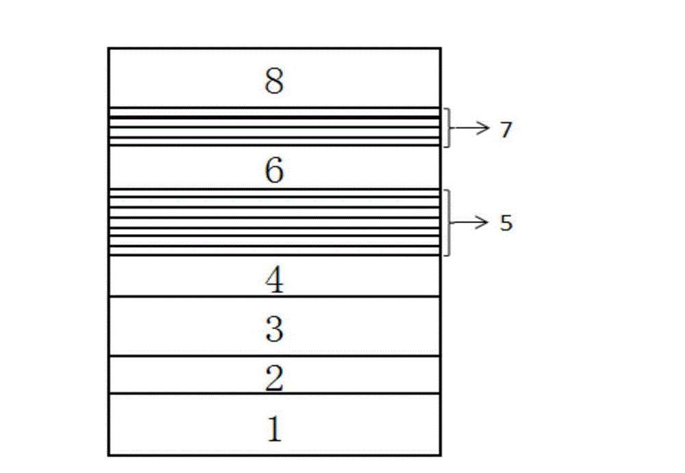
[0042] See structure figure 1 , taking the preparation of a P-type superlattice structure on a silicon carbide substrate by metal-organic chemical vapor deposition as an example, including the following steps:

[0043] (1) The silicon carbide substrate 1 is placed in the reaction chamber of a metal organic chemical vapor deposition (MOCVD) device, heated to 1050° C. under a hydrogen atmosphere, and processed for 15 minutes.

[0044] (2) An aluminum nitride nucleation layer 2 is grown on a silicon carbide substrate 1 at a growth temperature of 1000° C., a thickness of 150 nm, and a growth pressure of 50 torr.

[0045] (3) A non-doped gallium nitride layer (buffer layer) 3 is grown on the aluminum nitride nucleation layer 2 at a growth temperature of 1100° C., a growth thickness of 2 μm, and a growth rate of 2 μm / h.

[0046] (4) N-type gallium nitride 4 is grown on the galliu...

Embodiment 2

[0053] See structure figure 1 , taking the preparation of a P-type superlattice structure on a sapphire substrate by metal-organic chemical vapor deposition as an example, including the following steps:

[0054] (1) The sapphire substrate 1 is put into the reaction chamber of the metal organic chemical vapor deposition furnace (MOCVD) equipment, heated to 1000° C. under a hydrogen atmosphere, and processed for 12 minutes.

[0055] (2) An AlGaN nucleation layer 2 is grown on a sapphire substrate 1 at a growth temperature of 900° C., a thickness of 120 nm, and a growth pressure of 70 mbar.

[0056] (3) A non-doped GaN layer (buffer layer) 3 is grown on the AlGaN nucleation layer 2 at a growth temperature of 1100° C., a growth thickness of 2 μm, and a growth rate of 2 μm / h.

[0057] (4) N-type gallium nitride 4 is grown on the gallium nitride buffer layer 3, and the silicon doping concentration is 4×10 18 / cm -3 , with a thickness of 2 μm. The growth temperature is about 900°...

Embodiment 3

[0064] See structure figure 1 , taking the preparation of a gallium nitride-based light-emitting diode containing a P-type superlattice on a sapphire substrate as an example, including the following steps:

[0065] (1) The sapphire substrate 1 is put into the reaction chamber of the metal organic chemical vapor deposition furnace (MOCVD), heated to 1000° C. under a hydrogen atmosphere, and processed for 20 minutes.

[0066] (2) Growing gallium nitride nucleation layer 2 on sapphire substrate 1 . The growth temperature is 600° C., and the thickness is 50 nm. The growth pressure was 300 mbar.

[0067] (3) A non-doped gallium nitride layer 3 is grown on the gallium nitride nucleation layer 2 at a growth temperature of 1050° C., a growth thickness of 1.5 μm, and a growth rate of 3 μm / h.

[0068] (4) N-type gallium nitride 4 is grown on the gallium nitride buffer layer 3, and the silicon doping concentration is 3×10 18 / cm -3 , with a thickness of 2.5 μm. The growth temperatu...


PUM

PropertyMeasurementUnit
Thicknessaaaaaaaaaa
Thicknessaaaaaaaaaa
Thicknessaaaaaaaaaa

Abstract

The invention relates to an LED extension structure with P type superlattice and a preparation method thereof. The LED extension structure orderly comprises the following parts from the lower side to the upper side: a substrate, a nucleating layer, a buffer layer, n type GaN layer, a multiple quantum well luminescent layer, a first P type GaN layer, P type AlInN/GaN superlattice and a second P type GaN layer; the P type AlInN/GaN superlattice is composed of the AlInN potential well layer and GaN barrier layer overlapped periodically. The AlInN/GaN superlattice structure is adopted for effectively raising the hole concentration, effectively resisting the electron and useful for expanding the hole, the mismatch of the structure lattice is little, the crystal quality is high after growing. The GaN-based LED with P type structure containing AlInN/GaN superlattice can effectively improve the luminous efficiency of the device.

Description

technical field [0001] The invention belongs to the field of optoelectronics, and relates to an LED epitaxial structure with a P-type superlattice and a preparation method thereof. Background technique [0002] Gallium nitride material has a series of advantages such as wide band gap, high electron mobility, high thermal conductivity, high stability, etc. Power devices have a wide range of practical applications and huge market prospects. Light-emitting diodes (LEDs) have the advantages of small size, high efficiency, and long life. They are widely used in full-color displays, backlights, and signal lights, and have gradually become a research hotspot in the field of electronic power. [0003] P-type doping is an essential and important part of manufacturing GaN LED devices. Due to the passivation effect of Mg, when p-type GaN is grown by MOCVD technology, the acceptor Mg atoms are severely damaged by H (hydrogen atoms) during the growth process. Passivation, resulting in ...

Claims


Application Information

Patent Timeline
IPC IPC(8): H01L33/06H01L33/14H01L33/00
CPCH01L33/04H01L33/0066H01L33/0075H01L33/06H01L33/145H01L2933/0008
Inventor 逯瑶王成新曲爽马旺王志强
Owner SHANDONG INSPUR HUAGUANG OPTOELECTRONICS
Why Eureka
Try Eureka