
Preparation method of fast recovery diode

A recovery diode and field plate technology, which is used in semiconductor/solid-state device manufacturing, electrical components, circuits, etc., can solve the problems of long manufacturing cycle of fast recovery diode chips, complex fast recovery diode processes, and increased product cost, and achieves improved field performance. The effect of improving the quality of the board, reducing the surface contamination and improving the yield

Active Publication Date: 2015-05-13
BEIJING MXTRONICS CORP +1
View PDF6 Cites 6 Cited by
  • Summary
  • Abstract
  • Description
  • Claims
  • Application Information

AI Technical Summary

Problems solved by technology

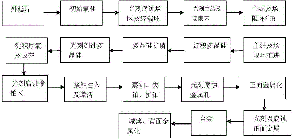
The process flow of the traditional diode preparation method is as follows: figure 1 As shown, the traditional manufacturing of the fast recovery diode terminal makes the manufacturing cycle of the fast recovery diode chip very long, thereby making the process of the fast recovery diode complicated and increasing the product cost

Method used


Image

  • Preparation method of fast recovery diode
  • Preparation method of fast recovery diode
  • Preparation method of fast recovery diode

Examples


Embodiment Construction

[0029] Below in conjunction with accompanying drawing and specific embodiment the present invention is described in further detail:

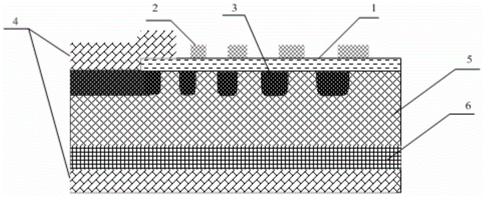
[0030] In the prior art, such as figure 1 The process flow shown, the structure diagram of the prepared fast recovery diode is as follows figure 2 As shown, it includes metal electrode 4 , polysilicon field plate 2 , PN junction P-type region 3 , field oxygen 1 , N-type epitaxial layer 5 and N-type heavily doped layer 6 .

[0031] Such as image 3 The flow chart of the preparation method of the present invention shown, the preparation method of a kind of fast recovery diode that this invention provides comprises the following steps:

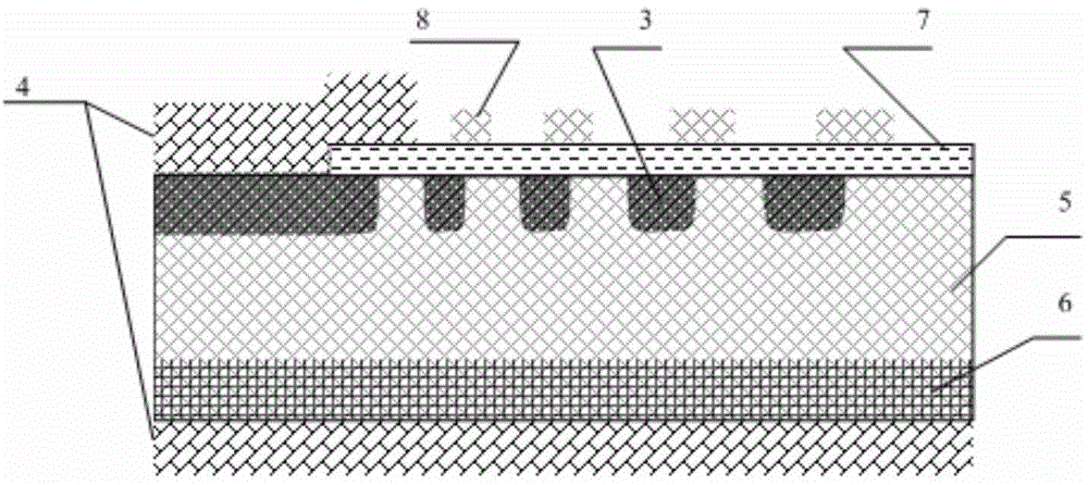
[0032] (1), using SOI epitaxial wafers as substrates, such as Figure 4 The schematic diagram of the structure of the SOI substrate shown, the SOI epitaxial wafer is sequentially composed of an N-type heavily doped layer 6, an N-type epitaxial layer 5, an SOI intermediate layer 7 and an upper silicon field plat...


PUM


Abstract

The invention provides a preparation method of a fast recovery diode; the method employs a SOI substrate to replace the conventional epitaxial wafer, and employs a planar manufacturing technology; the preparation method is compatible to the conventional fast recovery diode, and the method utilizes the silicon dioxide and the upper silicon in the SOI substrate as the field oxide and the field plate; due to the fact that the silicon dioxide in the SOI substrate is formed by absolutely pure oxygen atom injection, the silicon dioxide purity is high and in good contact with the lower silicon crystal, thus well reducing the surface pollution of the fast recovery diode, reducing the formation of surface charge, thereby reducing electric leakage on the surface, increasing the electric property and rate of finished product of the fast recovery diode; the preparation method of the fast recovery diode employs the SOI substrate to replace the conventional epitaxial wafer, thus reducing the manufacturing steps of the fast recovery diode, improving the quality of the field oxide and the polycrystalline silicon field plate, greatly reducing the charge of oxide layer interface, and increasing the consistency of the technology.

Description

technical field [0001] The invention relates to the technical field of power semiconductor devices, in particular to a preparation method of a fast recovery diode. Background technique [0002] Fast Recovery DiodeFast Recovery Diode (FRD for short), as a new type of power device that has come out in recent years, is one of the most used power semiconductor devices in power electronic equipment. Due to its good switching performance, short reverse recovery time, and large forward current , small size, easy installation and other advantages, it is often used in parallel with three-terminal power switching devices (such as IGBT, etc.) Market demand. From the perspective of withstand voltage range, FRDs between 400V and 1200V, which are mainly used in induction cookers, power supplies, frequency conversion appliances, frequency conversion welding machines, electric vehicles, etc. Widely used in industrial products such as appliances. The continuous development of power elect...

Claims


Application Information

Patent Timeline
Patent Type & Authority Applications(China)
IPC IPC(8): H01L21/329
CPCH01L29/6609
Inventor 冯幼明
Owner BEIJING MXTRONICS CORP
Learn More