Microfluidic chip bonding method using SU-8 photoresist and PDMS as substrates

A microfluidic chip, SU-8 technology, applied in microstructure technology, microstructure device, manufacturing microstructure device and other directions, can solve the problem of difficult bonding between SU-8 substrate and PDMS substrate, expensive and controllable equipment used It can solve problems such as poor stability and poor bonding effect, so as to achieve the effect of mature processing technology, less leakage and high yield

Active Publication Date: 2015-05-20
SOUTHEAST UNIV
View PDF6 Cites 8 Cited by
  • Summary
  • Abstract
  • Description
  • Claims
  • Application Information

AI Technical Summary

Problems solved by technology

[0005] In view of the above-mentioned shortcomings of the prior art, the purpose of the present invention is to provide a microfluidic chip bonding method using SU-8 photoresist and PDMS as the substrate, which is used to solve the problem of SU-8 substrate in the prior art. Difficult bonding of chips and PDMS substrates, high yield, expensive equipment and poor controllability, poor bonding effect, and easy leakage

Method used


Image

  • Microfluidic chip bonding method using SU-8 photoresist and PDMS as substrates
  • Microfluidic chip bonding method using SU-8 photoresist and PDMS as substrates
  • Microfluidic chip bonding method using SU-8 photoresist and PDMS as substrates

Examples


Embodiment Construction

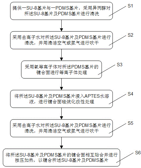
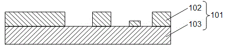
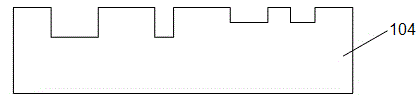
[0035] Embodiments of the present invention are described below through specific examples, and those skilled in the art can easily understand other advantages and effects of the present invention from the content disclosed in this specification. The present invention can also be implemented or applied through other different specific implementation modes, and various modifications or changes can be made to the details in this specification based on different viewpoints and applications without departing from the principle of the present invention.

[0036] see Figure 1~Figure 7 . It should be noted that the diagrams provided in this embodiment are only illustrative to illustrate the basic principles, working process and effects of the present invention, so that only components related to the present invention are shown in the diagrams rather than according to actual implementation The number, formation and dimension drawing of components, the type, quantity and ratio of each...


PUM


Abstract

The invention provides a microfluidic chip bonding method using an SU-8 photoresist and PDMS as substrates. The microfluidic chip bonding method comprises the following steps: firstly providing an SU-8 substrate and a PDMS substrate, cleaning the SU-8 substrate and the PDMS substrate by using isopropyl alcohol and deionized water, and then performing oxygen plasma treatment on the bonding surface of the PDMS substrate; performing silanization modification treatment on the bonding surfaces of the SU-8 substrate and the PDMS substrate by using an aqueous solution of APTES; and finally, enabling the bonding surfaces of the SU-8 substrate and the PDMS substrate to get close and carrying put press heating to bond the SU-8 substrate and the PDMS substrate to form a complete microfluidic chip. The microfluidic chip bonding method has the following beneficial effects that: 1) the bonding surface of the PDMS substrate can be modified by using an ordinary low-power plasma machine or a corona discharge instrument and other low-cost equipment; 2) the operation process is simple, the controllability, stability and repeatability of the process are high, the bonding strength and the yield are high, and the leakage does not easily occur; 3) the bonding of the SU-8 substrate and the PDMS substrate is helpful for realizing the precision multifunctional microfluidic chip with and complicated structure.

Description

technical field [0001] The invention provides a microfluidic chip bonding method using SU-8 photoresist and PDMS as substrates. It belongs to the field of microfluidic chips. technical background [0002] Microfluidics is a new research and application field interdisciplinary in biology, chemistry, medicine, physics, electronics, materials, machinery and so on. Microfluidic chip, also known as Lab-on-a-chip (Lab-on-a-chip), is a chip that integrates the basic operation units of sample preparation, reaction, separation, and detection in the process of biological, chemical, and medical analysis into a micro-nano scale. superior. The microfluidic chip forms a network with microchannels and microstructures, runs through the entire system with controllable fluids, and replaces various functions of conventional biological, chemical, and medical analysis laboratories to realize the miniaturization, portability, and multifunction of analytical equipment change. Microfluidic chip...

Claims


Application Information

Patent Timeline
Patent Type & Authority Applications(China)
IPC IPC(8): B81C1/00
Inventor 朱真
Owner SOUTHEAST UNIV
Why Eureka
Try Eureka