Graphene nanoelectronic device and preparation method thereof

A technology of electronic devices and graphene, which is applied in semiconductor/solid-state device manufacturing, electrical components, nanotechnology, etc., can solve the problems that cannot meet the needs of nanoelectronic device processing, graphene multilayer superposition of metal ions, nanometer size uncontrollable, etc. problems, to achieve the effect of good consistency, large grain size and wide application range

Active Publication Date: 2017-12-26
INST OF PHYSICS - CHINESE ACAD OF SCI
View PDF4 Cites 0 Cited by
  • Summary
  • Abstract
  • Description
  • Claims
  • Application Information

AI Technical Summary

Problems solved by technology

[0005] Although the above-mentioned method can obtain a porous graphene structure, and obtains good application prospects in some fields, some of the above-mentioned methods have the problem of uncontrollable nanometer size in the process of preparing the graphene structure, and the graphite obtained by some methods There are various problems such as multilayer stacking or metal ion pollution, which cannot meet the needs of nanoelectronic device processing.

Method used


Image

  • Graphene nanoelectronic device and preparation method thereof
  • Graphene nanoelectronic device and preparation method thereof
  • Graphene nanoelectronic device and preparation method thereof

Examples


preparation example Construction

[0032] In one embodiment of the present invention, the preparation method of graphene nanoelectronic device comprises:

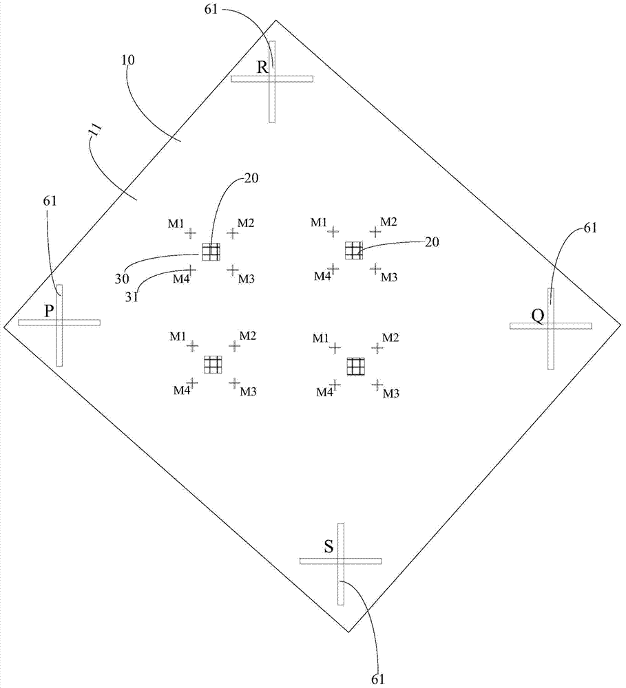
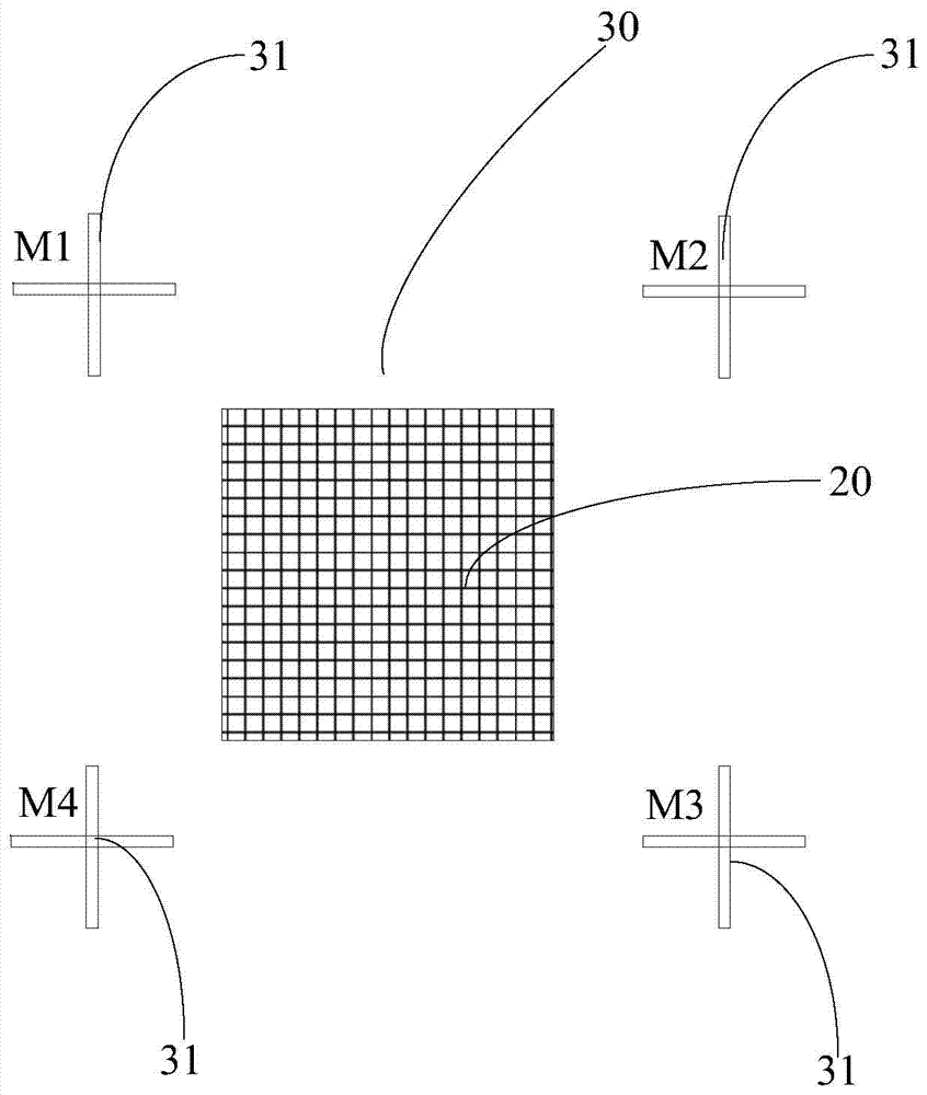
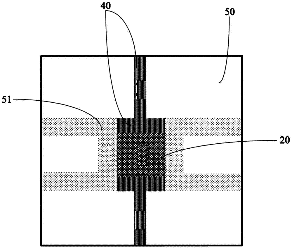
[0033] Step S1 , providing a substrate 10 . The upper surface 11 of the substrate 10 may be formed of an insulating dielectric material. A four-inch or larger wafer can also be selected as the insulating dielectric substrate 10 . The preparation method of the graphene nano-electronic device provided by the present invention does not have too much selectivity for the substrate material, and either an insulating dielectric substrate or a substrate of other materials, such as a conductive material, can be used as the substrate. The insulating dielectric substrate 10 can be a dielectric substrate such as wafer high-resistance or low-resistance silicon wafer, quartz wafer, sapphire wafer, silicon nitride wafer, silicon carbide wafer, lanthanum aluminate, gallium nitride, aluminum nitride, diamond wafer, etc. , it can also be a thin-film dielectric layer (such a...


PUM

PropertyMeasurementUnit
thicknessaaaaaaaaaa
thicknessaaaaaaaaaa
diameteraaaaaaaaaa

Abstract

The invention discloses a graphene nano-electronical appliance and a preparation method of the graphene nano-electronical appliance. The preparation method of the graphene nano-electronical appliance comprises the following steps: S1 providing a substrate of which upper surface is insulating medium material; S2, forming a continuous graphene layer on the upper surface, wherein the graphene layer can basically cover the whole upper surface of the substrate; S3, forming every metal electrode on the graphene layer; S4, covering a slushing compound layer on the graphene layer, and exposing the slushing compound layer by adopting an electronic beam, so that the slushing compound layer is shaped to be a preset mask shape; the mask pattern is shaped at a predetermined position of every graphene zone in the graphene layer to form a nano structure of every graphene zone; step S5, performing reaction ion etching on the substrate with the mask so as to form the nano structure; S6, removing a part of graphene layer at surrounding of the graphene zone, and disconnecting the graphene zone in the graphene layer from the other graphene layer out of the graphene zone. The method can prepare the graphene nano-electronical appliance with high precision and consistence on a large scale.

Description

technical field [0001] The invention relates to the technical field of micro-nano processing, in particular to a graphene nanoelectronic device and a preparation method thereof. Background technique [0002] Graphene is a quasi-two-dimensional nanomaterial composed of a single layer of carbon atoms, which has excellent physical, chemical and mechanical properties. Therefore, the current research on the material properties, preparation methods and device processing technology of graphene has become a hot spot. The preparation methods of graphene include many kinds, such as mechanical exfoliation method, silicon carbide pyrolysis method, arc discharge method and CVD synthesis method, etc. In the field of electronic device preparation, doping is of great help to improve and enhance the electrical and magnetic properties of graphene. For graphene with a two-dimensional structure, chemical doping has disadvantages such as difficult doping and poor stability. Physical structure...

Claims


Application Information

Patent Timeline
Patent Type & Authority Patents(China)
IPC IPC(8): H01L21/04H01L29/16B82Y10/00
CPCB82Y10/00H01L21/04H01L21/0405H01L29/16H01L29/1606
Inventor 唐成春顾长志杨海方李俊杰金爱子姜倩晴
Owner INST OF PHYSICS - CHINESE ACAD OF SCI
Why Eureka
Try Eureka