Vertically-oriented self-assembled segmented copolymer film, and production method and application thereof

A technology of block copolymer and vertical orientation, which is applied in the field of block copolymer thin film preparation, and can solve problems such as difficult and complex electrode structures

Active Publication Date: 2015-08-12
INST OF CHEM CHINESE ACAD OF SCI
View PDF1 Cites 2 Cited by
  • Summary
  • Abstract
  • Description
  • Claims
  • Application Information

AI Technical Summary

Problems solved by technology

However, this method of building an electric field has a complex electrode structure and requires a block polymer film with a micron-level thickness to facilitate electrode construction and separation. It is difficult to use this method in a film system with a thickness of na

Method used


Image

  • Vertically-oriented self-assembled segmented copolymer film, and production method and application thereof
  • Vertically-oriented self-assembled segmented copolymer film, and production method and application thereof
  • Vertically-oriented self-assembled segmented copolymer film, and production method and application thereof

Examples


Embodiment 1

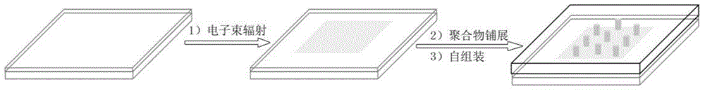
[0054] figure 1 Shown as a schematic diagram of a method for controlling the self-assembly structure of a vertically-oriented PS-b-PMMA film.

[0055] (1) Electron beam radiation

[0056] The electron beam has an acceleration voltage of 5kV, an electron beam current of 16.7pA, a radiation time of 6min (360s), and a radiation area of ​​11.32μm 2 (I.e. the radiation dose is 53mC / cm 2 ) Irradiate the surface of the silicon substrate containing the spontaneous oxide layer.

[0057] (2) Block copolymer spreading

[0058] The PS-b-PMMA (46k-b-21k) solution with a concentration of 9 mg / ml was spin-coated on the silicon substrate after electron beam irradiation at 2000 rpm for 40 seconds.

[0059] (3) Polymer self-assembly

[0060] The substrate containing the PS-b-PMMA film was annealed in a tube furnace at 250°C under Ar atmosphere for 2 hours, cooled to room temperature, and self-assembly was completed.

[0061] Finally, the annealed film was etched by argon plasma (20sccm, 50W, 5min), and the...

Embodiment 2

[0065] (1) Electron beam radiation

[0066] The electron beam has an acceleration voltage of 5kV, an electron beam current of 16.7pA, a radiation time of 3min, and a radiation area of ​​11.32μm 2 (I.e. the radiation dose is 26.5mC / cm 2 ) Irradiate the surface of a silicon substrate containing an artificial oxide layer.

[0067] (2) Block copolymer spreading

[0068] The PS-b-PMMA (53k-b-54k) solution with a concentration of 11 mg / ml was spin-coated on the silicon substrate after electron beam irradiation at 2000 rpm and 40 seconds.

[0069] (3) Polymer self-assembly

[0070] The substrate containing the PS-b-PMMA film was annealed in a tube furnace at 250°C under Ar atmosphere for 2 hours and cooled to room temperature to complete the self-assembly.

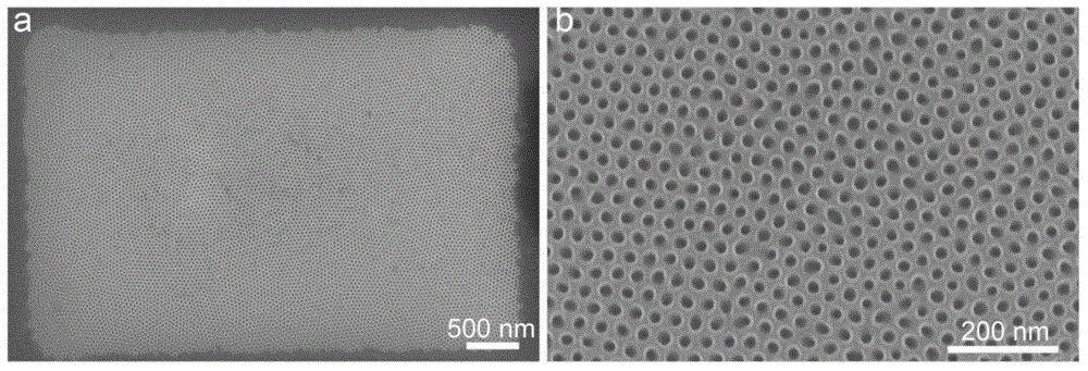
[0071] After processing according to the method of Example 1, the surface morphology was observed with a scanning electron microscope. Figure 4 It is the surface topography of the layered PS-b-PMMA film obtained in Example 2. The formed f...

Embodiment 3

[0073] (1) Electron beam radiation

[0074] The acceleration voltage of the electron beam is 5kV, the electron beam current is 16.7pA, and the radiation dose of the electron beam is 50mC / cm 2 The radiation area is a circular area with a diameter of 100 nm that radiates the surface of the silicon substrate containing the spontaneous oxide layer.

[0075] (2) Block copolymer spreading

[0076] A PS-b-PMMA (46k-b-21k) solution with a concentration of 9 mg / ml was spin-coated on the silicon substrate after electron beam irradiation at 2000 rpm for 40 seconds.

[0077] (3) Polymer self-assembly

[0078] The substrate containing the PS-b-PMMA film was annealed in a tube furnace at 250°C under Ar atmosphere for 2 hours and cooled to room temperature to complete the self-assembly.

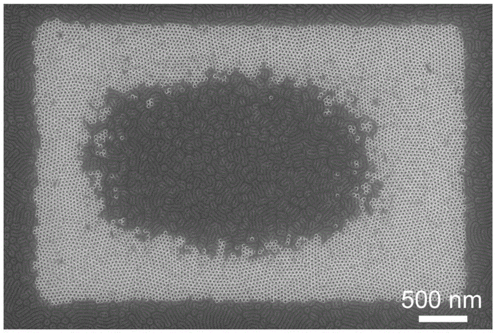
[0079] After processing according to the method of Example 1, the surface morphology was observed with a scanning electron microscope. Figure 5 It is the surface topography of the PS-b-PMMA film with the columnar str...


PUM


Abstract

The invention discloses a control method for forming a vertically-oriented assembly structure of a segmented copolymer. The segmented copolymer comprises multiple polystyrene-b-polymethacrylate (PS-b-PMA) different in molecular weight and segment proportion. The control method for vertical orientation includes evenly spreading a PS-b-PMA film on a substrate, subjected to electron beam radiation, with a low-electroconductivity or insulated surface and performing heating and annealing to obtain the segmented copolymer. The control method for vertical orientation of the PS-b-PMA has the advantages that novelty is high, operation process is simple, personalized patterns can be formed, interface regulation and control layers are not needed and macroscopic large-area morphology and microcosmic small-area morphology can be regulated and controlled accurately.

Description

Technical field [0001] The invention belongs to the field of macromolecular self-assembly, and more specifically, relates to a method for preparing a vertically-oriented self-assembled block copolymer film and its products and uses. Background technique [0002] Nano-patterning technology based on block polymer films, because block polymers can be assembled into small and controllable sizes (5-100nm), adjustable structures (spherical, columnar, layered, etc.), easy to achieve large-area assembly, etc. A series of advantages have become an effective method of surface patterning. This nano-patterning technology based on block polymer films has shown potential application prospects in the fields of microelectronic devices, magnetic energy storage devices, and porous filter membranes. [0003] In order to realize the application of block polymer-based nano-etching, the morphological orientation of the film needs to be controlled to obtain a vertically-oriented layered or columnar stru...

Claims


Application Information

Patent Timeline
IPC IPC(8): C08J5/18C08F299/00
Inventor 王栋武美玲万立骏
Owner INST OF CHEM CHINESE ACAD OF SCI
Why Eureka
Try Eureka