Method for manufacturing near-stoichiometry PPLN all-optical wavelength converter low in Mg doping

A near-stoichiometric ratio, wavelength converter technology, applied in the field of optical communications, can solve the problems of no anti-photorefractive characteristics, low conversion efficiency, small frequency multiplication nonlinear coefficient, etc., and achieve good anti-photorefractive characteristics , reduce the cost of raw materials, improve the effect of device integration

Inactive Publication Date: 2015-09-02
TIANJIN UNIV
View PDF6 Cites 10 Cited by
  • Summary
  • Abstract
  • Description
  • Claims
  • Application Information

AI Technical Summary

Problems solved by technology

[0004] After searching the literature of the prior art, it was found that the Chinese patent "Manufacturing Method of Wavelength-Tunable Broadband All-Optical Wavelength Converter" (patent number: ZL200510027943.4) belongs to the cascade effect of single-pump frequency multiplication and difference frequency, and has the following disadvantages : First, the non-linear coefficient of frequency doubling is not large, and a high pump light power is required to obtain considerable conversion efficiency, which is inconsistent with the low pump power threshold required in optical communication; second, the signal light and converted light are distributed in the pump Both sides of the pump light, so at least one wavelength channel is occupied, which is not conducive to the full utilization of the communication band; moreover, in the single pump wavelength conversion scheme, when the signal light wavelength approaches the pump light wavelength, the conversion efficiency will decrease. sag, so some channels near the pump wavelengt...

Method used


Image

  • Method for manufacturing near-stoichiometry PPLN all-optical wavelength converter low in Mg doping
  • Method for manufacturing near-stoichiometry PPLN all-optical wavelength converter low in Mg doping
  • Method for manufacturing near-stoichiometry PPLN all-optical wavelength converter low in Mg doping

Examples


Embodiment Construction

[0030] Specific embodiments of the present invention will be described in detail below in conjunction with the accompanying drawings. If there are exemplary contents in these embodiments, they should not be construed as limiting the present invention.

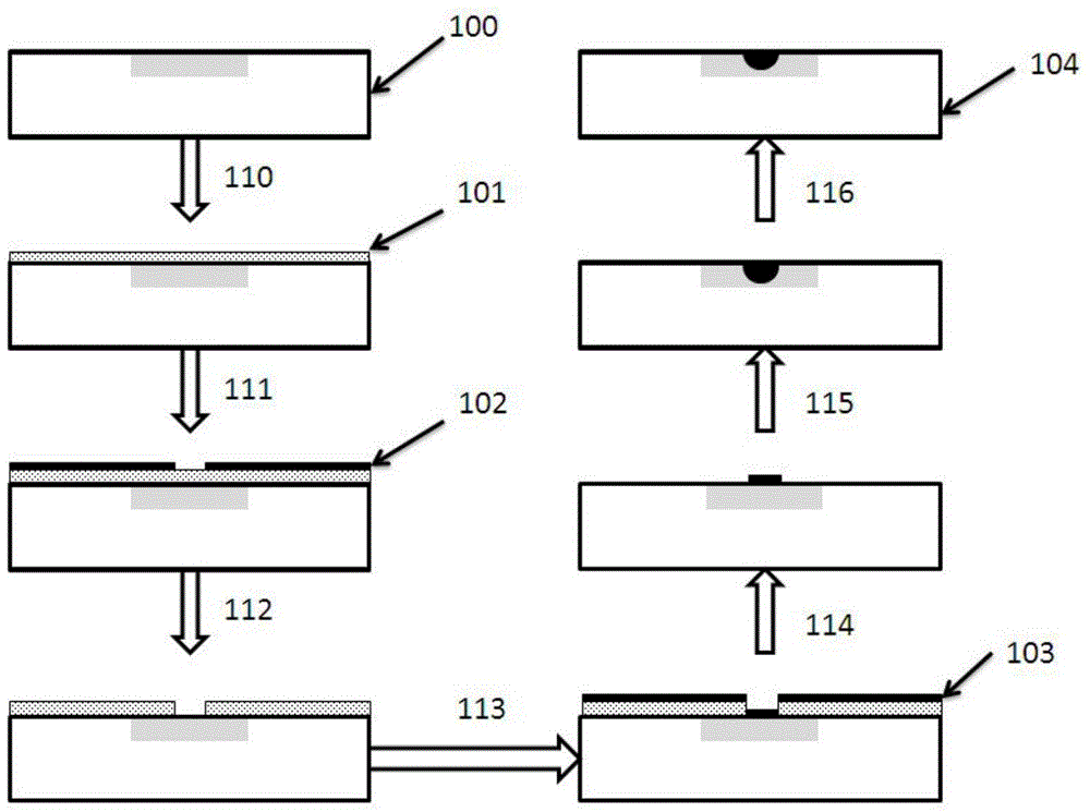
[0031] Step 1. Select a lithium niobate wafer of the same composition with a Z-cut thickness of 0.5mm-1mm. The upper and lower surfaces are parallel and both are optically polished. The normal direction of the upper and lower surfaces is the spontaneous polarization direction of the crystal;

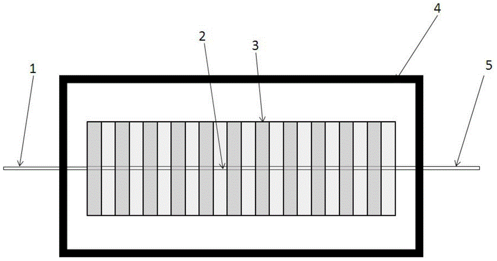
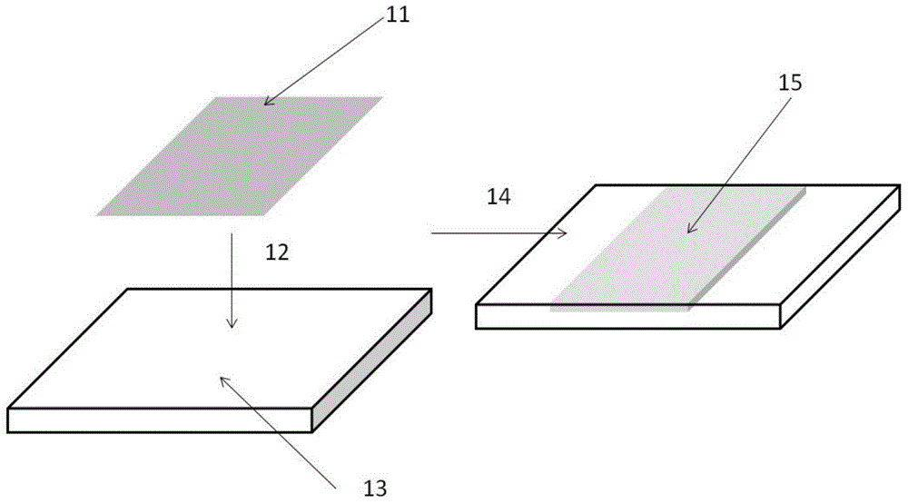
[0032] Step 2, Mg local doping: Coating a layer of MgO film on the surface of the wafer-Z, diffusing at a high temperature of 1050-1130°C for more than 1 hour to obtain lithium niobate crystals partially doped with magnesium, such as figure 2 shown;

[0033] Step 3. Manufacturing process of titanium-diffused lithium niobate optical waveguide: use photolithography process on the surface of the wafer-Z, plate titanium strips of 4-10 μm, us...


PUM


Abstract

The invention discloses a method for manufacturing a near-stoichiometry PPLN all-optical wavelength converter low in Mg doping. The method comprises the steps that firstly, a Z-cut congruent lithium niobate chip with two faces polished is selected, and after the -Z surface of the chip is locally doped with magnesium, a Ti diffusion strip optical waveguide is manufactured on the -Z surface of the chip doped with Mg; secondly, periodical polarization is conducted on the +Z surface of the chip, a periodical array metal optical grating electrode composed of a long aluminum strip is formed, a near-stoichiometry lithium niobate crystal doped with Mg is obtained by means of the rich-lithium VTE technique, and liquid polarization is conducted on the crystal at the indoor temperature by means of a liquid electrode polarization device, so that a periodical crystal superlattice is obtained; finally, the obtained product is doped with Mg, the PPLN crystal is packaged, and near-stoichiometry PPLN all-optical wavelength converter low in Mg doping is obtained. Compared with the prior art, the method has the advantages that cost is low, the use conditions and the application fields of the wavelength converter are widened, the wavelength converter can be integrated with other devices easily, the degree of integration of the devices is improved, coupling losses and transmission losses are greatly reduced, and the system stability is high.

Description

technical field [0001] The invention relates to the technical field of optical communication, in particular to a manufacturing method of an all-optical wavelength converter. Background technique [0002] Existing wavelength conversion devices mainly include cross-gain modulation and cross-phase modulation wavelength converters and Mach-Zehnder wavelength converters based on semiconductor optical amplifiers (SOA), but they are not completely transparent to the amplitude, frequency and phase of the input signal. conversion; and wavelength converter based on SOA or passive waveguide: although the four-wave mixing of optical fiber is a completely transparent all-optical conversion, but because it is a third-order nonlinear process, there is a problem of low conversion efficiency; in addition, this This kind of wavelength converter is noisy and easily causes crosstalk, so its application is limited. In general, the second-order nonlinear process is much more efficient than the t...

Claims


Application Information

Patent Timeline
IPC IPC(8): G02F1/35G02F2/00
CPCG02F1/3515G02F1/353G02F2/004G02F2203/58G02F2/006
Inventor 华平壤陈朝夕
Owner TIANJIN UNIV
Why Eureka
Try Eureka