Diamond-base double-layer insulated gate dielectric field effect transistor and a preparation method thereof

A field-effect transistor and double-layer insulation technology, which is applied in the manufacture of semiconductor/solid-state devices, semiconductor devices, electrical components, etc., can solve the problems affecting the direct current and microwave characteristics of field-effect transistors, the instability of surface adsorbates, and the limited application , to achieve the effect of maintaining hole density and carrier mobility, enhancing gate control ability, and reducing gate leakage current

Active Publication Date: 2015-10-21
XI AN JIAOTONG UNIV
View PDF2 Cites 22 Cited by
  • Summary
  • Abstract
  • Description
  • Claims
  • Application Information

AI Technical Summary

Problems solved by technology

However, the instability of surface adsorbates leads to the degradation or even failure of surface 2DHG performance under high temperature

Method used


Image

  • Diamond-base double-layer insulated gate dielectric field effect transistor and a preparation method thereof
  • Diamond-base double-layer insulated gate dielectric field effect transistor and a preparation method thereof
  • Diamond-base double-layer insulated gate dielectric field effect transistor and a preparation method thereof

Examples


Embodiment 1

[0065] A method for preparing a diamond-based double-layer insulated gate dielectric field effect transistor comprises the following steps:

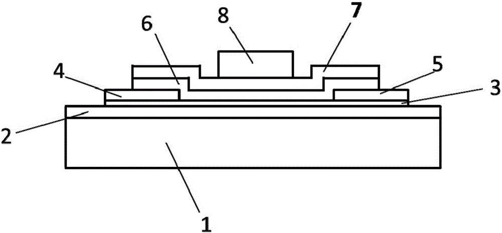
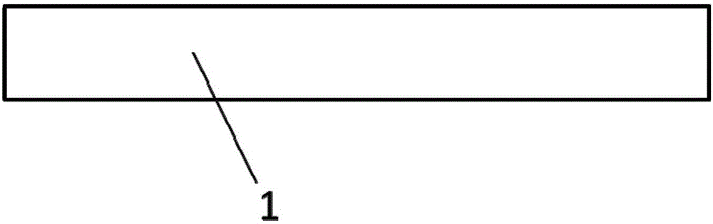
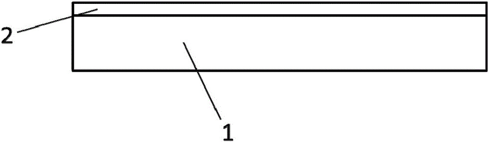
[0066] 1) The diamond substrate 1 grown by high temperature and high pressure (HPHT) technology is cleaned successively by using the standard cleaning process for diamond substrates, followed by inorganic and organic cleaning, and blown dry with nitrogen gas for later use.

[0067] 2) Deposit a single crystal diamond film 2 on the cleaned diamond substrate using microwave plasma vapor chemical deposition (MPCVD), the plasma power is 1kW, the chamber pressure is 100Torr, and the total gas flow is 500sccm, and the obtained single crystal diamond The thickness of the film is 1 μm, the resistivity is greater than 100MΩ cm, the root mean square (RMS) surface roughness is 0.3nm, and the half-peak width of the Raman curve is about 2cm -1 .

[0068] 3) Control the microwave plasma power so that the chamber temperature is 900° C., keep the hydroge...

Embodiment 2

[0074] A method for preparing a diamond-based double-layer insulated gate dielectric field effect transistor comprises the following steps:

[0075] 1) The diamond substrate 1 grown by high temperature and high pressure (HPHT) technology is cleaned successively by using the standard cleaning process for diamond substrates, followed by inorganic and organic cleaning, and blown dry with nitrogen gas for later use.

[0076] 2) Deposit a single crystal diamond film on the cleaned diamond substrate using hot wire chemical vapor deposition (HFCVD). The plasma power is 1kW, the chamber pressure is 100Torr, and the total gas flow is 500sccm. The thickness of the obtained single crystal diamond film is 1μm, the resistivity is greater than 100MΩ cm, the root mean square (RMS) surface roughness is about 0.3nm, and the half-peak width of the Raman curve is about 2cm -1 .

[0077] 3) Control the microwave plasma power so that the chamber temperature is 900°C, keep the hydrogen flow rate a...

Embodiment 3

[0083] A method for preparing a diamond-based double-layer insulated gate dielectric field effect transistor comprises the following steps:

[0084] 1) Use the standard diamond substrate cleaning process to perform inorganic and organic cleaning on the diamond substrate grown by high temperature and high pressure (HPHT) technology, and dry it with nitrogen gas for later use.

[0085] 2) Use microwave plasma vapor chemical deposition (MPCVD) technology to deposit single crystal diamond film on the diamond substrate after cleaning. The thickness is 1μm, the resistivity is greater than 100MΩ cm, the root mean square (RMS) surface roughness is 0.3nm, and the half-peak width of the Raman curve is about 2cm -1 .

[0086] 3) Control the microwave plasma power so that the chamber temperature is 900°C, keep the hydrogen flow rate at 50 sccm, and perform hydrogenation treatment on the grown single crystal epitaxial film. The treatment time is about 5 minutes, and the 2DHG areal density...


PUM

PropertyMeasurementUnit
Resistivityaaaaaaaaaa
Thicknessaaaaaaaaaa
Thicknessaaaaaaaaaa

Abstract

The invention discloses a diamond-base double-layer insulated gate dielectric field effect transistor (FET) and a preparation method thereof. The FET comprises a diamond substrate, a monocrystalline diamond epitaxial film, a conductive channel, a source electrode, a drain electrode, a first insulated gate dielectric layer, a second insulated gate dielectric layer, and a gate electrode. The diamond substrate is equipped with a layer of amonocrystalline diamond epitaxial film. The monocrystalline diamond epitaxial film is provided with the source electrode and the drain electrode. The conductive channel is formed in the monocrystalline diamond epitaxial film between the source electrode and the drain electrode. The first insulated gate dielectric layer covers the conductive channel between the source electrode and the drain electrode, and a part of the source electrode and the drain electrode. The second insulated gate dielectric layer is arranged on the first insulated gate dielectric layer. The gate electrode is arranged on the second insulated gate dielectric layer. The double-layer insulated gate dielectric structure effectively improves the DC and microwave characteristics of the FET.

Description

【Technical field】 [0001] The invention belongs to the field of semiconductor devices, in particular to a diamond-based field effect transistor and a preparation method thereof. 【Background technique】 [0002] Semiconductor single crystal materials have gone through four generations of development. The first generation of Si and Ge semiconductors brought mankind into the information age, and at the same time drove the intelligence and informatization of electronic systems. The second-generation semiconductors (GaAs, InP, MCT, etc.) have brought us optoelectronic devices, power electronic devices, radio frequency electronic devices, and space radiation-resistant devices, which have triggered revolutions in information fields such as wireless communications and optical communications. The third-generation wide-bandgap semiconductors (GaN, SiC) can partially meet the requirements of the new generation of electronic systems for semiconductor devices at high frequency (microwave-...

Claims


Application Information

Patent Timeline
IPC IPC(8): H01L29/78H01L29/423H01L29/66H01L21/04
CPCH01L21/044H01L29/42364H01L29/66969H01L29/78
Inventor 王玮王宏兴胡超李奉南李硕业刘璋成张景文卜忍安侯洵
Owner XI AN JIAOTONG UNIV
Why Eureka
Try Eureka