Low temperature polycrystalline silicon thin film, thin film transistor and respective manufacturing method and display device

A low-temperature polysilicon and thin film transistor technology, which is applied in transistors, semiconductor/solid-state device manufacturing, electric solid-state devices, etc. Effect of grain size improvement, grain boundary position improvement, and electrical properties improvement

Active Publication Date: 2015-11-25
BOE TECH GRP CO LTD
View PDF6 Cites 10 Cited by
  • Summary
  • Abstract
  • Description
  • Claims
  • Application Information

AI Technical Summary

Problems solved by technology

[0004] Although low-temperature polysilicon thin film transistors have the above-mentioned advantages, the low-temperature polysilicon thin film (that is, the active layer) in low-temperature polysilicon thin-film transistors (LTPSTFT) is formed by laser annealing of amorphous silicon thin films, while laser annealing The process will cause non-uniform grain size of polysilicon and very large roughness on the surface of polysilicon film, which will lead to poor uniformity of threshold voltage and mobility of low-temperature polysilicon thin film transistors, especially when the transistor size shrinks, the threshold voltage The problem of unevenness will become more serious

Method used


Image

  • Low temperature polycrystalline silicon thin film, thin film transistor and respective manufacturing method and display device
  • Low temperature polycrystalline silicon thin film, thin film transistor and respective manufacturing method and display device
  • Low temperature polycrystalline silicon thin film, thin film transistor and respective manufacturing method and display device

Examples


Embodiment 1

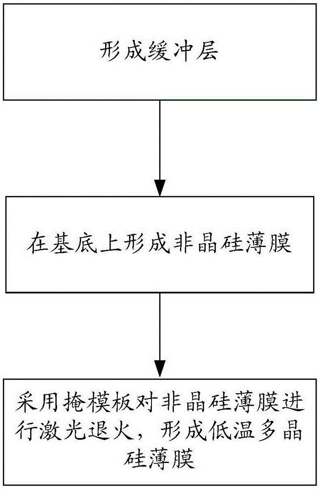
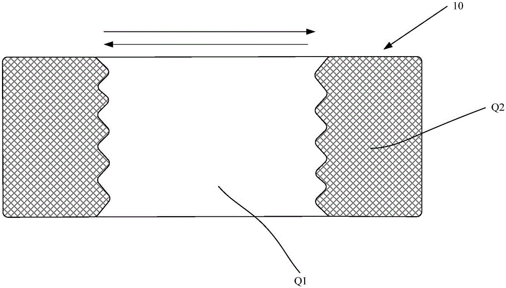
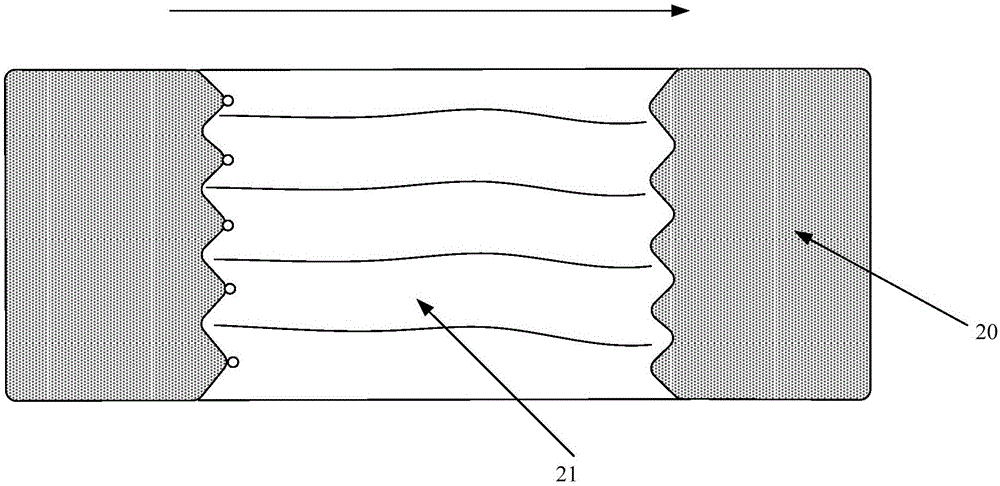
[0044] Such as Figure 1-3 As shown, this embodiment provides a method for preparing a low-temperature polysilicon thin film, comprising the following steps:

[0045] Step 1, forming a buffer layer on the substrate.

[0046] In this step, the substrate is made of a transparent material such as glass and is pre-cleaned. Specifically, sputtering, thermal evaporation, plasma enhanced chemical vapor deposition (PlasmaEnhancedChemicalVaporDeposition: PECVD for short), low pressure chemical vapor deposition (LowPressureChemicalVaporDeposition: LPCVD for short), atmospheric pressure chemical vapor deposition (AtmosphericPressureChemicalVaporDeposition: APCVD) or electron cyclotron resonance chemical vapor deposition (Electron Cyclotron Resonance Chemical Vapor Deposition: ECR-CVD for short) to form the buffer layer.

[0047] Wherein, the buffer layer includes at least one layer of silicon oxide and silicon nitride. In addition, the thickness of the buffer layer may be 150nm to 300...

Embodiment 2

[0060] Such as Figure 4 , 5 As shown, this embodiment provides a method for preparing a low-temperature polysilicon thin film transistor, which includes the steps of preparing a low-temperature polysilicon thin film described in Embodiment 1. Specifically, the preparation of a top-gate transistor is taken as an example for illustration.

[0061] Step 1, forming a buffer layer on the substrate.

[0062] In this step, the substrate is made of a transparent material such as glass and is pre-cleaned. Specifically, a buffer layer is formed on the substrate 1 by sputtering, thermal evaporation, plasma enhanced chemical vapor deposition, low pressure chemical vapor deposition, atmospheric pressure chemical vapor deposition or electron cyclotron resonance chemical vapor deposition.

[0063] Wherein, the buffer layer includes at least one layer of silicon oxide and silicon nitride, with a thickness of 150nm to 300nm. The reason for preparing such a thick buffer layer is to form an...

Embodiment 3

[0085] This embodiment provides a display device, which includes the above-mentioned low-temperature polysilicon thin film transistor, so the display effect of the display device of this embodiment is better.

[0086] The display device can be any product or component with a display function such as a liquid crystal panel, an electronic paper, an OLED panel, a mobile phone, a tablet computer, a television, a monitor, a notebook computer, a digital photo frame, a navigator, and the like.


PUM

PropertyMeasurementUnit
thicknessaaaaaaaaaa

Abstract

The invention provides a low temperature polycrystalline silicon thin film, a thin film transistor and respective manufacturing method and a display device, belongs to the technical field of display, and can solve the problem of poor uniformity of the existing low temperature polycrystalline silicon thin film. The manufacturing method of the low temperature polycrystalline silicon thin film comprises: forming an amorphous silicon thin film above a substrate; and performing laser annealing on the amorphous silicon thin film by adopting a mask plate to form the low temperature polycrystalline silicon thin film, wherein the mask plate comprises a photic zone and a shading zone surrounded by the photic zone, and two opposite sides of the shading zone are of a fluctuant structure. The performance of the low temperature polycrystalline silicon thin film formed by the manufacturing method is improved.

Description

technical field [0001] The invention belongs to the field of display technology, and in particular relates to a low-temperature polysilicon thin film, a thin film transistor, their respective preparation methods, and a display device. Background technique [0002] With the development of display technology, people's demand for display quality is increasing day by day, and the demand for high-quality, high-resolution flat panel display devices is becoming more and more common, and more and more attention has been paid by display panel manufacturers. [0003] A thin film transistor (Thin Film Transistor, TFT for short) is a main driving device of a flat panel display panel, and is directly related to the development direction of a high-performance flat panel display device. Thin film transistors have various structures, and there are also various materials for preparing thin film transistors with corresponding structures. For example, amorphous silicon and polysilicon are curr...

Claims


Application Information

Patent Timeline
Patent Type & Authority Applications(China)
IPC IPC(8): H01L21/02H01L21/336H01L29/786
CPCH01L21/0268H01L21/02488H01L21/02532H01L21/02592H01L27/1222H01L27/1285H01L27/1288H01L29/04H01L29/66757H01L29/78675H01L29/78696H01L29/6675H01L29/78672
Inventor 李栋陆小勇李小龙刘政张帅詹裕程刘建宏龙春平
Owner BOE TECH GRP CO LTD
Why Eureka
Try Eureka