Organic thin-film solar cell based on dual cathode buffer layers and preparation method of organic thin-film solar cell
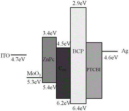
A cathode buffer layer, solar cell technology, applied in circuits, photovoltaic power generation, electrical components, etc., can solve problems such as changing exciton quenching and carrier transport, reduce energy level barriers, optimize energy level matching, The effect of improving collection efficiency
- Summary
- Abstract
- Description
- Claims
- Application Information
AI Technical Summary
Problems solved by technology
Method used
Image
Examples
Embodiment 1
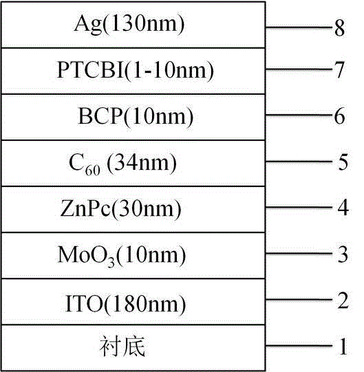
[0042] The structure of organic solar cells such as figure 1 shown. The material, thickness and doping ratio of each layer of the device are as follows: the transparent substrate is glass, the transparent anode electrode is ITO, and the thickness is 180nm; the anode modification layer is MoO 3, the thickness is 10nm; the donor layer is ZnPC, the thickness is 30nm; the acceptor layer is C 60 , with a thickness of 34nm; the first electron buffer layer is BCP, with a thickness of 10nm; the second cathode modification layer is PTCBI, with a thickness of 1nm; the cathode electrode is Ag, with a thickness of 130nm.
[0043] Its preparation method is as follows:
[0044] ① The glass substrate on which the transparent anode electrode ITO has been sputtered is ultrasonically cleaned with detergent, deionized water, acetone solution and ethanol solution, and dried with dry nitrogen after cleaning;
[0045] ② Move the above-mentioned ITO substrate into a vacuum chamber, and conduct pl...
Embodiment 2
[0053] The structure of organic solar cells such as figure 1 shown. The material, thickness and doping ratio of each layer of the device are as follows: the transparent substrate is glass, the transparent anode electrode is ITO, and the thickness is 180nm; the anode modification layer is MoO 3 , the thickness is 10nm; the donor layer is ZnPC, the thickness is 30nm; the acceptor layer is C 60 , with a thickness of 34nm; the first electron buffer layer is BCP, with a thickness of 10nm; the second cathode modification layer is PTCBI, with a thickness of 2nm; the cathode electrode is Ag, with a thickness of 130nm. The preparation process is basically similar to Example 1.
Embodiment 3
[0055] The structure of organic solar cells such as figure 1 shown. The material, thickness and doping ratio of each layer of the device are as follows: the transparent substrate is glass, the transparent anode electrode is ITO, and the thickness is 180nm; the anode modification layer is MoO 3 , the thickness is 10nm; the donor layer is ZnPC, the thickness is 30nm; the acceptor layer is C 60 , with a thickness of 34nm; the first electron buffer layer is BCP, with a thickness of 10nm; the second cathode modification layer is PTCBI, with a thickness of 3nm; the cathode electrode is Ag, with a thickness of 130nm. The preparation process is basically similar to Example 1.
PUM
| Property | Measurement | Unit |
|---|---|---|
| Thickness | aaaaa | aaaaa |
| Thickness | aaaaa | aaaaa |
| Thickness | aaaaa | aaaaa |
Abstract
Description
Claims
Application Information
 - R&D
- Intellectual Property
- Life Sciences
- Materials
- Tech Scout
- Unparalleled Data Quality
- Higher Quality Content
- 60% Fewer Hallucinations
Browse by: Latest US Patents, China's latest patents, Technical Efficacy Thesaurus, Application Domain, Technology Topic, Popular Technical Reports.
© 2025 PatSnap. All rights reserved.Legal|Privacy policy|Modern Slavery Act Transparency Statement|Sitemap|About US| Contact US: help@patsnap.com


