Conductor line and manufacture method thereof
A manufacturing method and conductor circuit technology, which are applied in printed circuit manufacturing, printed circuit, conductive pattern formation and other directions, can solve the problems of poor process environmental protection, affect the overall performance, low yield rate, etc., achieve good environmental protection, simple manufacturing process, The effect of high yield
- Summary
- Abstract
- Description
- Claims
- Application Information
AI Technical Summary
Problems solved by technology
Method used
Image

Examples
Embodiment 1
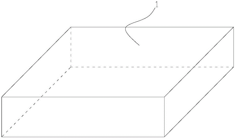
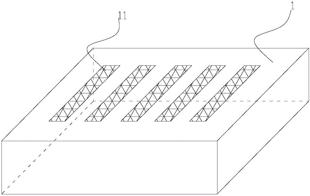
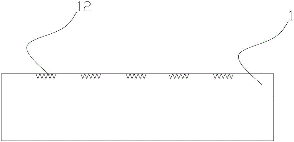
[0049] According to another aspect of the present invention, a method of manufacturing a conductor line is provided. Carriers can be selected as needed. It is usually a non-metallic carrier, such as plastic, plastic, glass or ceramics. In the present embodiment, the carrier adopts a plastic carrier 1, and the plastic carrier 1 is made of PC (polycarbonate), ABS (acrylonitrile-butadiene-styrene copolymer), PBT (polybutylene terephthalate), One or more materials in PES (polyethersulfone resin), PSU (polysulfone plastic) or GF (glass fiber), mixed with injection molding, extrusion or blow molding. In this embodiment, electroless plating is used for the plating treatment. Electroplating and other methods can also be used for plating treatment. refer to Figure 1-Figure 5 , including the following steps:
[0050] S1. Prepare a plastic carrier 1, and perform a first modification treatment on the plastic carrier 1 according to a set pattern, so as to form an uneven rough surface...
Embodiment 2
[0075] This embodiment provides a conductor circuit, which is manufactured according to the manufacturing method of the conductor circuit disclosed in the present invention. Including: carrier and conductor line body. The body of the conductor line is a combination of multiple metals or a metal. Commonly used conductive metals are copper, nickel, gold, silver or tin, or other conductive alloy materials or superconducting materials. Multiple metal materials can be deposited in layers to form a multilayer conductive material body. The conductor line body is embedded on the carrier. Commonly used carrier materials include plastics, plastics, glass, and ceramics. The carrier is modified to form an uneven rough surface area; the second modification is used to form a sensitized area; after activation, an activated area containing catalytic crystal nuclei is formed without adding a special catalyst to the carrier; the conductor circuit body It can be deposited on the carrier by el...
PUM
| Property | Measurement | Unit |
|---|---|---|
| Wavelength | aaaaa | aaaaa |
| Wavelength | aaaaa | aaaaa |
| Thickness | aaaaa | aaaaa |
Abstract
Description
Claims
Application Information
 - Generate Ideas
- Intellectual Property
- Life Sciences
- Materials
- Tech Scout
- Unparalleled Data Quality
- Higher Quality Content
- 60% Fewer Hallucinations
Browse by: Latest US Patents, China's latest patents, Technical Efficacy Thesaurus, Application Domain, Technology Topic, Popular Technical Reports.
© 2025 PatSnap. All rights reserved.Legal|Privacy policy|Modern Slavery Act Transparency Statement|Sitemap|About US| Contact US: help@patsnap.com