An Si-PIN four-quadrant photoelectric detector based on MEMS microstructure silicon and a manufacturing method thereof

A photodetector and microstructure technology, applied in the field of photoelectric detection, can solve the problem of inability to achieve precise positioning and target detection at the same time, and achieve the effect of widening the spectral response range, low cost and high responsivity

Inactive Publication Date: 2015-12-02
UNIV OF ELECTRONICS SCI & TECH OF CHINA
View PDF4 Cites 9 Cited by
  • Summary
  • Abstract
  • Description
  • Claims
  • Application Information

AI Technical Summary

Problems solved by technology

At this time, it is impossible to achieve precise positioning and target detection at the same time only relying on unit detectors

Method used


Image

  • An Si-PIN four-quadrant photoelectric detector based on MEMS microstructure silicon and a manufacturing method thereof
  • An Si-PIN four-quadrant photoelectric detector based on MEMS microstructure silicon and a manufacturing method thereof
  • An Si-PIN four-quadrant photoelectric detector based on MEMS microstructure silicon and a manufacturing method thereof

Examples


Embodiment 1

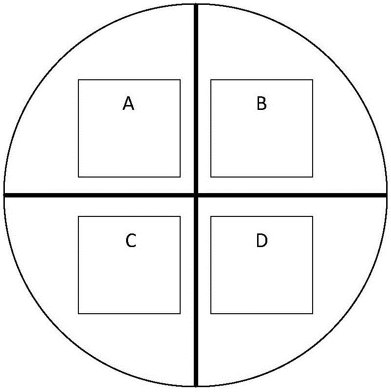
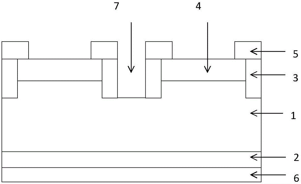
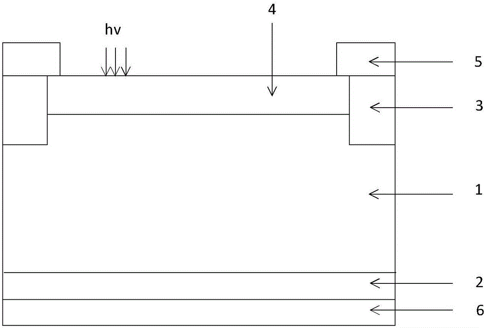
[0039] A Si-PIN four-quadrant photodetector based on MEMS microstructure silicon, including 4 unit photodetectors with identical performance located in different quadrants in Cartesian coordinates, characterized in that: the unit photodetectors are packaged sequentially from bottom to top The lower electrode 6, the N-type MEMS microstructure silicon layer 2, the silicon intrinsic substrate 1, the silicon intrinsic substrate 1 is provided with a P-type region 4, and an annular P + region 3, also includes a P-type region 4, and P + For the upper electrode 5 on the upper surface of the area 3, the surface of the MEMS microstructured silicon layer is columns or holes arranged in an array, with a diameter of 2 μm, a height or depth of 1 μm, and a period of 2 μm. Doping S or Te elements on MEMS microstructure silicon, ion implantation doping concentration range is 1×10 14 ion / cm 2 . The ring P + Region 3 is doped with boron B, and its doping concentration range is 1×10 18 ion / c...

Embodiment 2

[0041] A Si-PIN four-quadrant photodetector based on MEMS microstructure silicon, including four unit photodetectors with the same performance located in different quadrants in Cartesian coordinates, and the unit photodetectors are arranged sequentially from bottom to top. Electrode 6, N-type MEMS microstructure silicon layer 2, silicon intrinsic substrate 1, on which silicon intrinsic substrate 1 is provided with P-type region 4, and annular P + region 3, also includes a P-type region 4, and P + The upper electrode 5 on the upper surface of the region 3 . The surface of the MEMS microstructured silicon layer is columns or holes arranged in an array, with a diameter of 3 μm, a height or depth of 2 μm, and a period of 3 μm. Doping S or Te elements on MEMS microstructure silicon, ion implantation doping concentration range is 1×10 16 ion / cm 2 . The ring P + Region 3 is doped with boron B, and its doping concentration range is 5×10 19 ion / cm 3 . The upper end electrode 5 ...

Embodiment 3

[0043] A method for preparing a Si-PIN four-quadrant detector based on MEMS microstructure silicon, the steps are as follows:

[0044] Step 1: Prepare a silicon single wafer substrate material with a clean and dry surface, a high-resistance resistivity of 1000Ω·cm-2000Ω·cm, and a crystal orientation of , and oxidize and grow SiO on the surface of the silicon substrate 1 2 film layer.

[0045] Step 2: On SiO 2 Two quadrant isolation grooves are photoetched on the film layer along two orthogonal diameter directions, the groove width is 100 μm, and the groove depth is 3 μm.

[0046] Step 3: SiO in each quadrant 2 Synchronous photoetching of P around the surface of the film + The pattern of area 3, and then perform boron B heavy diffusion doping to form P + Zone 3, the doping concentration range is 1×10 18 ion / cm 3 .

[0047] Step 4: SiO in each quadrant 2 The pattern of the P-type region 4 is synchronously photoetched on the surface of the film layer, and then boron B is ...


PUM

PropertyMeasurementUnit
diameteraaaaaaaaaa
thicknessaaaaaaaaaa
thicknessaaaaaaaaaa

Abstract

An Si-PIN four-quadrant photoelectric detector based on MEMS microstructure silicon and a manufacturing method thereof belong to the technical field of photoelectric detection. The Si-PIN photoelectric detector of each quadrant of the four-quadrant photoelectric detector comprises a silicon intrinsic substrate 1, a P-type zone 4 positioned above the center of the front surface of the silicon intrinsic substrate, annular P+ zone 3 positions on the periphery above the center of the front surface of the silicon intrinsic substrate, an N-type MEMS microstructure silicon layer zone 2 Located below the silicon intrinsic substrate, upper electrodes 5 positioned on the both sides of the surface of the P type zone and P + zones and a lower electrode 6 positioned on the lower surface of the N-type MEMS microstructure silicon layer zone. Each unit detecting device is separated by an isolating groove, thereby effectively reducing signal crosstalk between small-quadrants. Compared with a traditional Si-PIN four-quadrant photoelectric detector, the Si-PIN four-quadrant photoelectric detector of the invention have characteristics of high responsibility, a broad responding wave band scope and a high between-quadrant signal-to-noise-ratio, etc. The function and the usage scope of the four-quadrant photoelectric detector can be expanded to satisfy demands of large scale marketization application.

Description

technical field [0001] The invention belongs to the technical field of photoelectric detection, and relates to a four-quadrant photodetection device structure, in particular to a front-illuminated Si-PIN four-quadrant photodetector based on MEMS microstructure silicon and a preparation method thereof. Background technique [0002] In laser ranging and optical communication technology, the optical signal receiving devices used are usually unit devices, such as PN junction diodes, PIN photodiodes and APD diodes, etc., but if the target to be detected is a moving object, such as a flying missile , its position will change with time. At this time, we not only need to know the distance of the target, but also know the orientation of the target. At this time, it is impossible to achieve precise positioning and target detection at the same time only relying on unit detectors. [0003] Four-quadrant photodetectors have the characteristics of high sensitivity and position resolution...

Claims


Application Information

Patent Timeline
Patent Type & Authority Applications(China)
IPC IPC(8): G01J1/42B81B7/00B81C1/00
Inventor 李伟盛浩钟豪卢满辉郭国辉蒋亚东
Owner UNIV OF ELECTRONICS SCI & TECH OF CHINA
Why Eureka
Try Eureka