Organic photoelectric detector with high external quantum efficiency and broad spectral response and preparation method thereof

A technology of external quantum efficiency and photodetectors, which is applied in photovoltaic power generation, electric solid-state devices, semiconductor/solid-state device manufacturing, etc., can solve the problems of wide response spectrum of difficult devices, reduction of external quantum efficiency, and low external quantum efficiency. Achieve the effect of improving the external quantum efficiency, high photoelectric multiplication effect, and improving the spectral response range

Active Publication Date: 2015-12-02
中科应化(长春)科技有限公司
View PDF3 Cites 13 Cited by
  • Summary
  • Abstract
  • Description
  • Claims
  • Application Information

AI Technical Summary

Problems solved by technology

In 2007, Perzon et al. synthesized the polymer LBPP-1. Due to its good absorption in the near-infrared region and good photoelectric properties, the spectral response range of the device can reach 1200nm, but the external quantum efficiency of the device is low. Its maximum external quantum efficiency is only 10%
In 2011, Binda et al. used a spin-coatable polymer as a barrier layer to prevent electrons from being injected from the anode into the organic layer, and successfully reduced the dark state current density of the devic...

Method used


Image

  • Organic photoelectric detector with high external quantum efficiency and broad spectral response and preparation method thereof
  • Organic photoelectric detector with high external quantum efficiency and broad spectral response and preparation method thereof
  • Organic photoelectric detector with high external quantum efficiency and broad spectral response and preparation method thereof

Examples


Embodiment 1

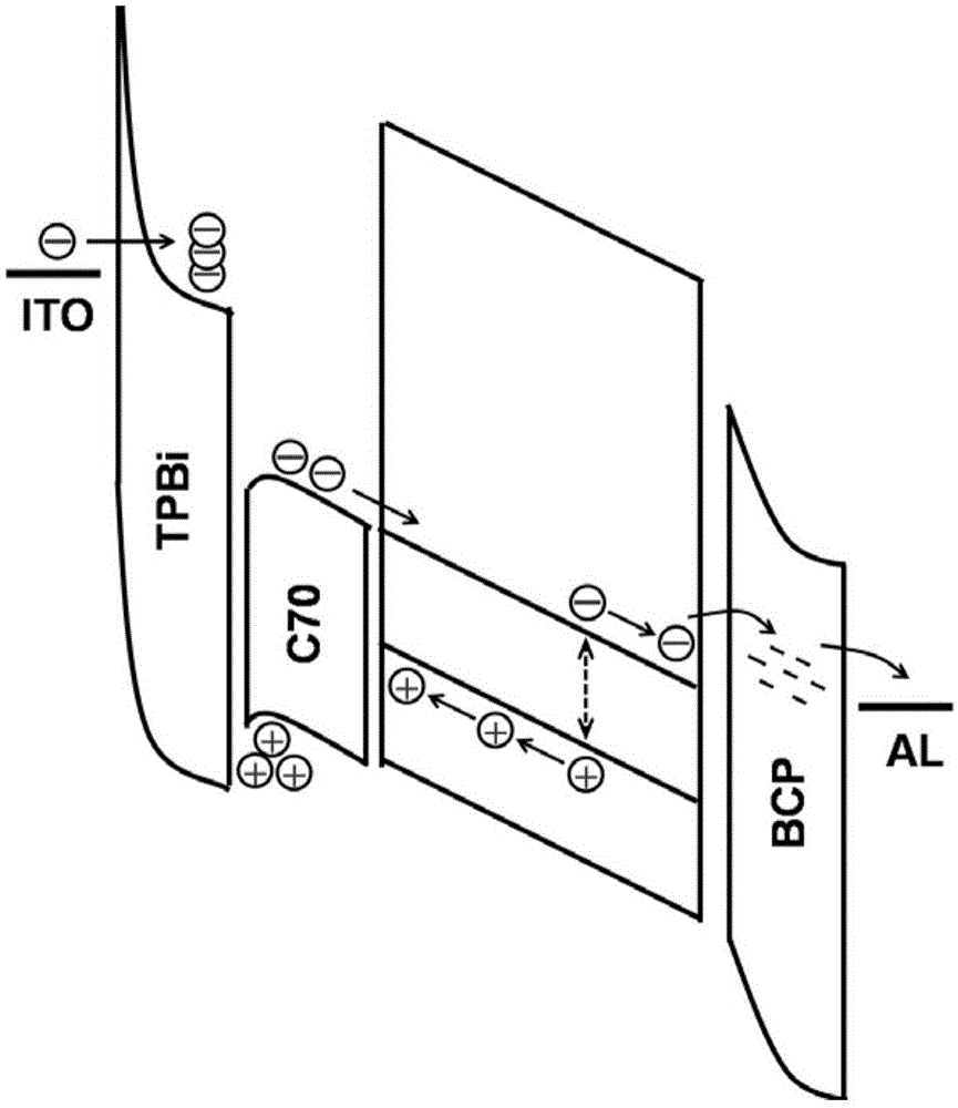
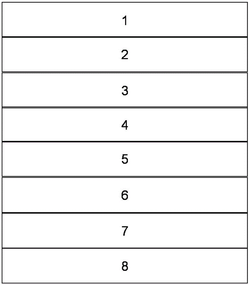
[0066] First, the ITO anode 3 on the glass substrate 2 is photoetched into an electrode with a width of 4 mm and a length of 30 mm, then cleaned, blown dry with nitrogen, and the glass is placed in a vacuum oven and baked at 110 degrees Celsius for 30 minutes. After plasma treatment for 2 minutes, the glass was placed in a vacuum coating system. When the vacuum degree of the vacuum coating system reaches 1 to 5×10 -4 At the time of Pascal, a layer of 4P-NPB was evaporated on the side of the glass without ITO, and then the electron injection barrier layer 4 (TPBi), the electron transport layer 5 (C70), and the active layer 6 (SnPc) were evaporated on the ITO layer in sequence. and C70 mixed layer), hole injection blocking layer 7 (BCP) and cathode 8 (Al), wherein the two electrodes cross each other to form the effective photodetection area of ​​the device, and its effective area is 16 square millimeters, and the injection blocking layer 4 The thickness is 3 nanometers, the thi...

Embodiment 2

[0069] First, the ITO anode 3 on the glass substrate 2 is photoetched into an electrode with a width of 4 mm and a length of 30 mm, then cleaned, blown dry with nitrogen, and the glass is placed in a vacuum oven and baked at 110 degrees Celsius for 30 minutes. After plasma treatment for 2 minutes, the glass was placed in a vacuum coating system. When the vacuum degree of the vacuum coating system reaches 1 to 5×10 -4 At the time of Pascal, a layer of 4P-NPB was evaporated on the side of the glass without ITO, and then the electron injection barrier layer 4 (TPBi), the electron transport layer 5 (C70), and the active layer 6 (SnPc) were evaporated on the ITO layer in sequence. and C70 mixed layer), hole injection blocking layer 7 (BCP) and cathode 8 (Al), wherein the two electrodes intersect each other to form the effective photodetection area of ​​the device, and its effective area is 16 square millimeters, and the injection blocking layer 4 The thickness is 3 nanometers, the...

Embodiment 3

[0072] First, the ITO anode 3 on the glass substrate 2 is photoetched into an electrode with a width of 4 mm and a length of 30 mm, then cleaned, blown dry with nitrogen, and the glass is placed in a vacuum oven and baked at 110 degrees Celsius for 30 minutes. After plasma treatment for 2 minutes, the glass was placed in a vacuum coating system. When the vacuum degree of the vacuum coating system reaches 1 to 5×10 -4 At the time of Pascal, a layer of 4P-NPB was evaporated on the side of the glass without ITO, and then the electron injection barrier layer 4 (TPBi), the electron transport layer 5 (C70), and the active layer 6 (SnPc) were evaporated on the ITO layer in sequence. and C70 mixed layer), hole injection blocking layer 7 (BCP) and cathode 8 (Al), wherein the two electrodes cross each other to form the effective photodetection area of ​​the device, and its effective area is 16 square millimeters, and the injection blocking layer 4 The thickness is 3 nanometers, the thi...


PUM

PropertyMeasurementUnit
Thicknessaaaaaaaaaa
Thicknessaaaaaaaaaa
Thicknessaaaaaaaaaa

Abstract

The present invention relates to an organic photoelectric detector with high external quantum efficiency and a broad spectral response. The organic photoelectric detector provided by the invention comprises the followings connecting in order: a lower conversion layer, a substrate, an anode, an electron injection barrier layer, an electron-transporting layer, an active layer and a cathode. The thickness of the electron injection barrier layer is from 1 nm to 10 nm, the thickness of the electron-transporting layer is from 5 nm to 60 nm, the thickness of the active layer is from 5 nm to 200 nm, and the thickness of the cathode is from 50 nm to 1000 nm. According to the invention, a relatively high photoelectric multiplication effect (EQE>15000%) is realized as well by means of improving the electron tunneling injection at electrodes through employing holes after exciton dissociation, and the structure provided by the invention is fully beneficial to an organic photoelectric detection device realizing a broad spectral response.

Description

technical field [0001] The invention relates to an organic photodetector, in particular to an organic photodetector with high external quantum efficiency and wide spectral response and a preparation method thereof. Background technique [0002] Organic photodetectors will find wide applications in consumer electronics, household appliances, smart building lighting, industry, production safety, health care and life sciences, environment, toys, and education due to their many advantages such as flexibility, cheapness, and ease of integration. Applications. To meet the requirements of practical applications, organic photodetectors should have high external quantum efficiency and wide spectral response range. At present, the spectral response range of organic photodetector devices is relatively narrow. In the ultraviolet band, due to the absorption of ultraviolet light by glass and ITO, the response of the device in the deep ultraviolet region is relatively small; in the near-...

Claims


Application Information

Patent Timeline
IPC IPC(8): H01L51/42H01L51/44H01L51/46H01L51/48
CPCH10K85/211H10K30/87H10K30/00Y02E10/549Y02P70/50
Inventor 马东阁杨德志
Owner 中科应化(长春)科技有限公司
Why Eureka
Try Eureka