A kind of silicon carbide-based semiconductor circuit breaker and its preparation method

A circuit breaker, silicon carbide technology, applied in the direction of semiconductor devices, circuits, electrical components, etc., can solve the problems of loss of pumping characteristics, loss of off-state characteristics, etc., achieve low on-resistance, reduce switching power consumption, and work reliably Effect

Active Publication Date: 2017-12-12
HUAZHONG UNIV OF SCI & TECH
View PDF4 Cites 0 Cited by
  • Summary
  • Abstract
  • Description
  • Claims
  • Application Information

AI Technical Summary

Problems solved by technology

[0003] However, further studies have shown that for silicon-based SOS semiconductor off-circuit switches, there are limitations in the optimization of parameters such as cut-off impedance, cut-off time, voltage gain, output pulse width at half maximum, and energy transfer efficiency, pumping characteristics and off-state The compromise between characteristics is limited by the silicon material, so that there is a limit to the overall performance. Improving the pumping characteristics will cause losses to the off-state characteristics, and improving the off-state characteristics will also cause losses to the pumping characteristics; in this case, In this field, there is an urgent need to find a more perfect semiconductor circuit breaker and its preparation method, so as to solve the above-mentioned problems of the prior art and obtain a semiconductor circuit breaker with higher comprehensive performance

Method used


Image

  • A kind of silicon carbide-based semiconductor circuit breaker and its preparation method
  • A kind of silicon carbide-based semiconductor circuit breaker and its preparation method
  • A kind of silicon carbide-based semiconductor circuit breaker and its preparation method

Examples


Embodiment 1

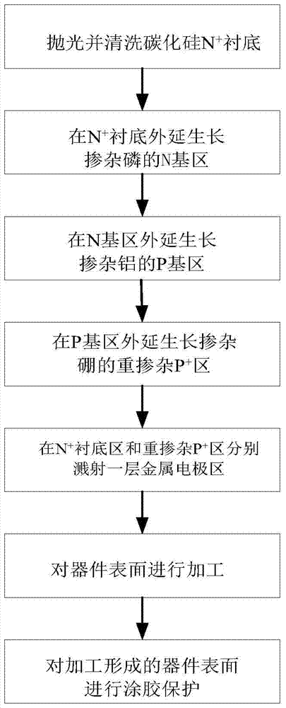
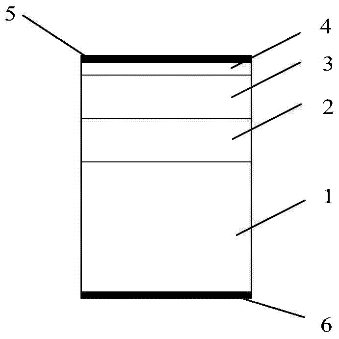
[0063] In Example 1, N + The thickness of the substrate is 300 μm; the concentration of phosphorus doped in the N base is 10 14 cm 3 , with a thickness of 10 μm; the concentration of doped aluminum in the P base region is 10 16 / cm 3 ~10 17 / cm 3 , and the concentration gradient is 9*10 14 / (cm 3 μm) incremental growth with a thickness of 100 μm; heavily doped P + region doped with boron at a concentration of 10 19 / cm 3 , with a thickness of 1 μm;

Embodiment 2

[0065] Example 2 according to figure 1 The illustrated process flow is used to complete the preparation of the silicon carbide-based semiconductor circuit breaker, the difference from Embodiment 1 is:

[0066] In step (2), the concentration of the N base region is controlled at 10 16 / cm 3 ~10 17 / cm 3 , and the concentration gradient is 9*10 14 / (cm 3 μm) incremental growth, with a thickness of 100 μm; under this parameter condition, when the switch PN junction is conducting forward, the accumulation of minority carriers on both sides of the space charge region, when the switch PN junction voltage reverses, can produce a large The reverse current realizes the SOS effect, which is beneficial to the miniaturization of the device;

[0067] And in step (3), the doping concentration of the P base region doped with aluminum is 10 14 / cm 3 ;

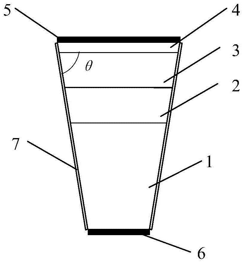
[0068] And in step (6), when the mesa is processed by mechanical cutting into an oblique angle, the PN junction is cut and penetrate...


PUM

PropertyMeasurementUnit
thicknessaaaaaaaaaa
thicknessaaaaaaaaaa
etching poweraaaaaaaaaa

Abstract

The invention discloses a manufacturing method for a semiconductor cut-out switch based on silicon carbide. The method comprises the following steps: using silicon carbide as an N+ substrate, a phosphorus-doped N base region, an aluminum-doped P base region, and a boron-doped heavy-doping P+ region epitaxially growing in sequence on the substrate; respectively processing two ends of the formed device to form a cathode electrode and an anode electrode; using a mechanical cutting oblique angle method to execute platform modeling and gumming protection, so as to complete a manufacturing process of the semiconductor cut-out switch. The invention also discloses a semiconductor cut-out switch based on silicon carbide, the switch being manufactured by the method. The semiconductor cut-out switch manufactured by the manufacturing method has larger compromise among pumping, switching, and switching characteristics, heat radiation requirement under a high-frequency condition is reduced, and reliability under high-temperature condition is improved.

Description

technical field [0001] The invention belongs to the technical field of semiconductor switches, and more specifically relates to a silicon carbide-based semiconductor circuit breaker and a preparation method thereof. Background technique [0002] Semiconductor opening switch SOS (Semiconductor Opening Switch) is a new type of solid switching device, which was first discovered in 1991 by S.K.Lyubutin and others from the Russian Institute of Electrophysics when they used high-voltage diodes (SDL) for rectification experiments. Forward current and reverse current (current density up to tens of kA / cm 2 , the current passing time is hundreds of ns) through p + -p-n-n + The structure of the semiconductor, the decay time of the reverse current is reduced to tens of ns. This phenomenon that the large current density is truncated in the nanosecond time is called the SOS effect. The compact all-solid-state high repetition frequency pulse power source based on SOS switch has the adv...

Claims


Application Information

Patent Timeline
Patent Type & Authority Patents(China)
IPC IPC(8): H01L29/24H01L29/861H01L29/06
CPCH01L29/0684H01L29/24H01L29/861
Inventor 梁琳舒玉雄
Owner HUAZHONG UNIV OF SCI & TECH
Why Eureka
Try Eureka