Guided mode resonance wave shifting device for scintillation detection

A technology of guided mode resonance and scintillation detection, which is applied in the field of nuclear radiation detection, can solve the problems of the difficulty in measuring fluorescence in the vacuum ultraviolet band, the inability to control the directionality of light emission, and low time resolution, and achieve good radiation resistance. Improving the time resolution ability and the effect of mature process conditions

Inactive Publication Date: 2015-12-30
TONGJI UNIV
View PDF1 Cites 12 Cited by
  • Summary
  • Abstract
  • Description
  • Claims
  • Application Information

AI Technical Summary

Problems solved by technology

In short, fluorescence measurement in the vacuum ultraviolet band is a difficult thing
[0003] Chinese patent CN1318537C discloses a rare earth-doped tantalate transparent luminescent film and its preparation method, the chemical expression of the transparent film is (Ln 1-x RE x )TaO 4 , where, 0
"AnovelM′-typeLuTaO 4 :Ln 3+ (Ln=Eu, Tb)transparentscintillatorfilms", XiaolinLiu, ShiweiChen, MuGu, MengqiuWu, ZhicheQiu, BoLiu, ChenNiandShimingHuang, OPTICALMATERIALSEXPRESSVol.4, No.1, p.172-178, also disclosed Eu 3+ The decay time of luminescence is 1.078 milliseconds, Tb 3+ The decay time of the luminescence is 1.096 milliseconds, so it can be seen that the time resolution of the above system is low

Method used


Image

  • Guided mode resonance wave shifting device for scintillation detection
  • Guided mode resonance wave shifting device for scintillation detection
  • Guided mode resonance wave shifting device for scintillation detection

Examples


Embodiment 1

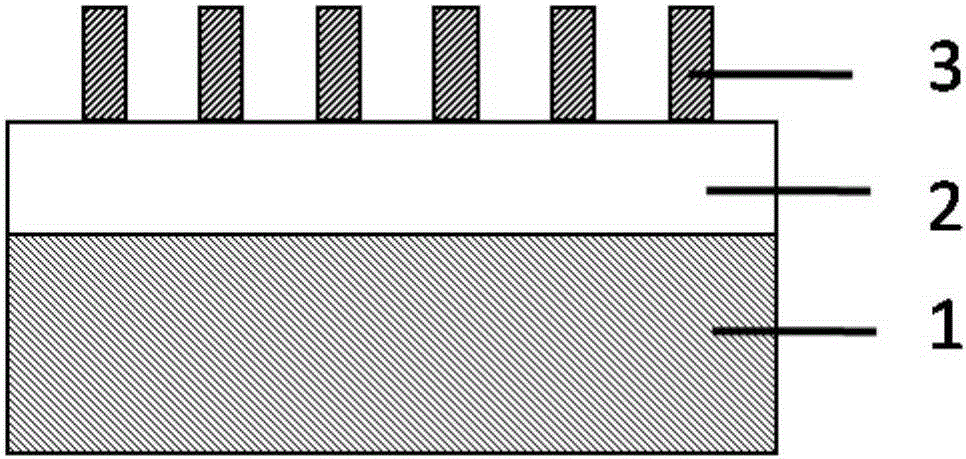
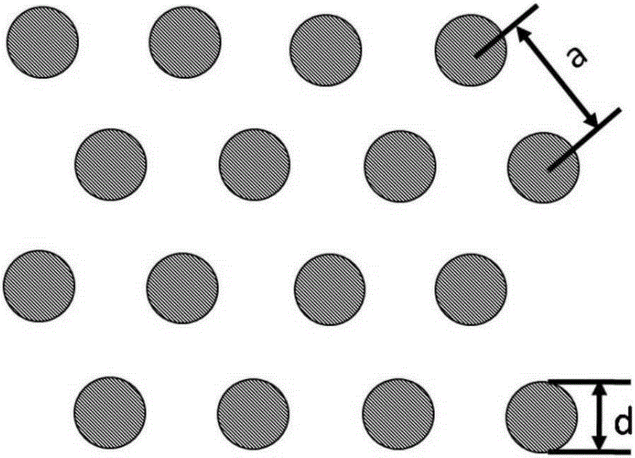
[0027] The structure diagram of the present invention is as figure 1 As shown, it includes a base layer 1, a luminescent film layer 2, and a photonic crystal layer 3. The luminescent film layer 2 is arranged on the base layer 1, and the photonic crystal layer 3 is arranged on the luminescent film layer. figure 2 It is a schematic diagram of the structure of the photonic crystal in the present invention, wherein a is the period of the periodic array of triangular configuration in the photonic crystal layer, and d is the diameter of the dielectric column.

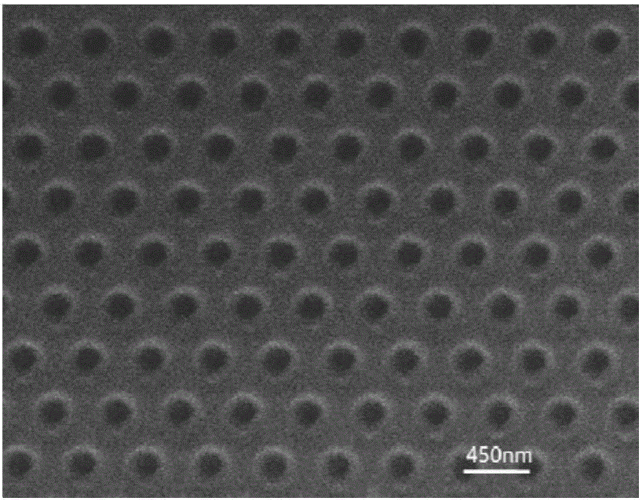
[0028] The selected material and structural parameters of this embodiment are as follows: select CaF 2 The crystal is the base layer, and the luminescent film layer is (Lu 0.9 Ce 0.1 ) 2 SiO 5 The thickness is chosen as The period of the photonic crystal is 430nm, the diameter of the dielectric column is 215nm, the height is 210nm, and the dielectric material is SiN.

[0029]The preparation process is as follows: (1) ...

Embodiment 2

[0031] The material and structural parameters selected in this embodiment are as follows: LiF crystal is selected as the base layer, and the luminescent film layer is (Lu 0.9 Ce 0.1 ) 2 SiO 5 The thickness is chosen as The period of the photonic crystal is 350nm, the diameter of the dielectric column is 175nm, the height is 210nm, and the dielectric material is SiN.

[0032] The sample preparation method is the same as in Example 1, except that the concentration of PEG400 used in the preparation of the luminescent film is reduced to obtain a film thickness of 159 nm. The pattern during electron beam exposure during photonic crystal preparation can be implemented according to the design parameters of this example.

[0033] Figure 5 It is the angle dependence of the luminescence spectrum of the sample under the excitation of far ultraviolet light. The results show that it has obvious emission at an angle of 36°, and the luminous intensity at this angle accounts for about ...

Embodiment 3

[0035] This embodiment is basically the same as Embodiment 1, the difference is that the diameter of the dielectric column of the photonic crystal layer is 236nm, the height of the dielectric column is 252nm, and the obtained guided mode resonance wave shifting device for scintillation detection has high conversion Efficiency and time resolution, and a high degree of light emission direction control ability, can improve the detection efficiency of ultraviolet and other scintillation fluorescence.


PUM

PropertyMeasurementUnit
heightaaaaaaaaaa
diameteraaaaaaaaaa
heightaaaaaaaaaa

Abstract

The invention relates to a guided mode resonance wave shifting device for scintillation detection. The guided mode resonance wave shifting device comprises a substrate layer and a luminous film layer arranged on the substrate layer, and also comprises a photonic crystal layer arranged on the luminous film layer, wherein the photonic crystal layer consists of dielectric cylinders arranged into a period array in a triangular structure; the dielectric cylinders are vertically arranged on the upper surface of the luminous film layer; the materials of the dielectric cylinders are transparent for the light emitted by the luminous film layer. Compared with the prior art, the guided mode resonance wave shifting device has the advantages that the conversion efficiency and the time distinguishing capability are high; high light emission direction regulation and control capability is also realized; the detection efficiency on scintillation fluorescence such as ultraviolet rays can be improved.

Description

technical field [0001] The invention belongs to the field of nuclear radiation detection, in particular to a guided-mode resonance wave-shifting device of a scintillation detection system. Background technique [0002] Scintillation detection is the most widely used detection method in nuclear radiation detectors. The emission wavelength of the scintillator determines the spectral response requirements of the detection and fluorescence transmission system. Some existing scintillators, such as inert gases such as Ar, He, Kr, and Xe, have scintillation peak wavelengths mainly in the vacuum ultraviolet band (105nm to 190nm) under radiation excitation. Because the fluorescence in the vacuum ultraviolet band puts forward special requirements for the detector, most of the existing optoelectronic devices such as photomultiplier tubes and semiconductor photonic devices do not respond to the fluorescence in the vacuum ultraviolet band. In short, fluorescence measurement in vacuum u...

Claims


Application Information

Patent Timeline
Patent Type & Authority Applications(China)
IPC IPC(8): G02F1/01G02F1/00
CPCG02F1/00G02F1/0009G02F1/0102
Inventor 刘波程传伟顾牡陈鸿黄世明刘小林
Owner TONGJI UNIV
Why Eureka
Try Eureka