InGaN/GaN multi-quantum-well single-nano-pole LED device and manufacturing method thereof

A technology of LED devices and multiple quantum wells, applied in semiconductor devices, electrical components, circuits, etc., can solve the problems that hinder the development and application of nano-devices, the processing technology cannot be realized, and the cost of preparing a single root is high, so as to weaken the influence and achieve successful production. High efficiency and high reliability

Active Publication Date: 2015-12-30
NANJING UNIV
View PDF5 Cites 10 Cited by
  • Summary
  • Abstract
  • Description
  • Claims
  • Application Information

AI Technical Summary

Problems solved by technology

[0005] Secondly, how to realize the electrical injection of nano-devices is another difficulty of this subject, which not only restricts the further research and exploration of its performance, but also hinders the development and application of nano-devices
At present, the patent document CN103077888A discloses a method for preparing electrodes on a single nanowire based on the electron beam exposure process. Nanowires are easy to peel off during peeling and other steps, so the yield is relatively low
The journal AppliedPhysicsLetter reported the preparation of InGaN / GaN multi-quantum well single nanocolumn LED devices by ultraviolet lithography, which showed good luminous characteristics, but the limitation of this single ultraviolet lithography technology lies in the diffraction limit, for less than 1 micron long single nanowire, this processing technology cannot achieve

Method used


Image

  • InGaN/GaN multi-quantum-well single-nano-pole LED device and manufacturing method thereof
  • InGaN/GaN multi-quantum-well single-nano-pole LED device and manufacturing method thereof
  • InGaN/GaN multi-quantum-well single-nano-pole LED device and manufacturing method thereof

Examples


Embodiment 1

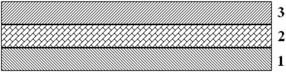
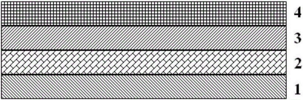
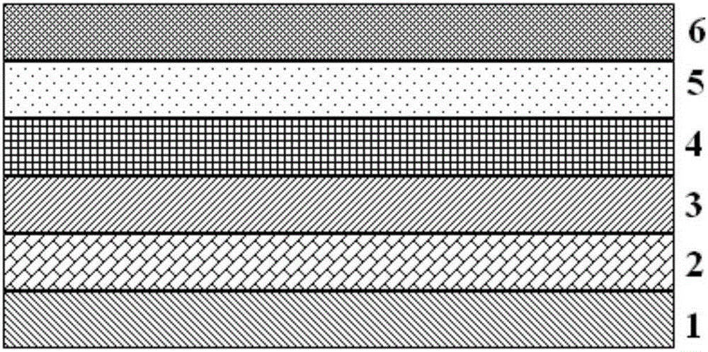
[0056] The InGaN / GaN multi-quantum well single nanocolumn LED device comprises:

[0057] A1. A 300nm-thick layer of SiO is grown on an InGaN / GaN multi-quantum well LED substrate with an In composition of 0.3, a luminous wavelength of 510nm, and a quantum well period of 10. 2 Insulation layer, 200nm thick PMMA glue and 30nm thick UV curing glue were spin-coated on SiO 2 The surface of the insulating layer; the thickness of the P-type GaN layer of the InGaN / GaN multi-quantum well LED substrate is 500nm, the thickness of the InGaN well layer is 3nm, the thickness of the GaN barrier layer is 12nm, and the thickness of the n-type GaN layer is 2um;

[0058] A2. Using UV soft nano-imprint technology, the soft template prepared in advance and treated with anti-adhesive treatment is in close contact with the surface of the UV-cured adhesive layer of the device, fully exposed to the UV lamp to cure the UV-cured adhesive, and then demoulded, so that The soft template is separated from t...

Embodiment 2

[0073] This InGaN / GaN multi-quantum well single nanocolumn LED device is made by the method of Example 1, the difference is that the device substrate is quartz, and the device insulating layer is SiO 2 layer, the thickness is 50nm, the period number of the InGaN / GaN quantum well active layer is 15, the In composition is 0.35, the emission wavelength is 550nm, the thickness of the p-type GaN layer is 300nm, and the thickness of the n-type GaN layer is 1.5μm , the diameter of the prepared nano-column is 500nm, the length is 3.5μm, the metal electrode film layer is Ni / Au / Ti / Au four-layer metal film obtained by electron evaporation deposition, the thickness is 500nm, the size of the Pt electrode is 400nm×400nm , with a deposition height of 500 nm.

Embodiment 3

[0075] This InGaN / GaN multi-quantum well single nanocolumn LED device is made by the method of embodiment 1, the difference is that the device substrate is PDMS, and the device insulating layer is SiO 2 layer, the thickness is 200nm, the period number of the InGaN / GaN quantum well active layer is 12, the In composition is 0.12, the emission wavelength is 430nm, the thickness of the p-type GaN layer is 400nm, and the thickness of the n-type GaN layer is 3μm, The diameter of the prepared nanocolumn is 70nm, the length is 0.8μm, the metal electrode film layer is a Ti / Au double-layer metal film obtained by electron evaporation deposition, the thickness is 200nm, the size of the Pt electrode is 200nm×200nm, and the deposition height is 200nm .


PUM


Abstract

The invention discloses an InGaN/GaN multi-quantum-well single-nano-pole LED device. The distance between an n-type GaN layer and a p-type GaN layer at the two ends of an InGaN/GaN multi-quantum-well nano-pole and the corresponding portions of a metal electrode film is smaller than or equal to 100 nm or the n-type GaN layer and the p-type GaN layer at the two ends of the InGaN/GaN multi-quantum-well nano-pole are in direct contact with the metal electrode film, a middle InxGa1-x/GaN quantum well active layer is isolated from the metal electrode film, and metal electrodes are secondarily deposited at the portions where the two ends of the InGaN/GaN multi-quantum-well nano-pole are in contact with the metal electrode film through a focused ion beam system to form ohmic contact. A method of the InGaN/GaN multi-quantum-well single-nano-pole LED device is mainly characterized in that ohmic contact of the nano-pole is formed through ultraviolet photoetching and focusing ion beam secondary depositing. By means of the method, the alignment accuracy between the electrodes and the nano-pole can be remarkably improved, the preparing success rate can be remarkably increased, multiple InGaN/GaN quantum wells are not damaged while the electrodes are prepared, good metal semiconductor contact is achieved accordingly, the electric injection current density is improved, and therefore luminance is improved. The method is suitable for preparing a single-nano-pole InGaN/GaN light emitting diode, and is particularly suitable for nanometer devices with the sizes smaller than the limitation of ultraviolet photoetching.

Description

technical field [0001] The invention relates to an InGaN / GaN multi-quantum well single nanocolumn LED device and a preparation method thereof, belonging to the field of semiconductor lighting. Background technique [0002] In recent years, low-dimensional quantum structures such as semiconductor nanowires / pillars and nanodots have attracted widespread attention from academic and industrial circles at home and abroad, hoping to exhibit special properties in mechanics, biochemistry, electromagnetism and optoelectronics, and in microscopic systems. Explore the carrier transport mechanism. Due to its high geometric confinement effect and novel functionality, nanoscale heterojunctions are developing rapidly in the field of optoelectronic devices, such as LED light-emitting diodes, lasers, solar cells, detectors, etc. Sub-wavelength light-emitting devices and high-polarization light sources are key factors in the development of light displays, especially in the development of hig...

Claims


Application Information

Patent Timeline
Patent Type & Authority Applications(China)
IPC IPC(8): H01L33/06H01L33/32H01L33/36H01L33/00
CPCH01L33/0066H01L33/0075H01L33/06H01L33/32H01L33/36H01L2933/0016
Inventor 刘斌智婷张荣陶涛谢自力郭旭葛海雄陈鹏陈敦军韩平施毅郑有炓
Owner NANJING UNIV
Why Eureka
Try Eureka