ZnO piezoelectric effect-based low-power consumption flexible resistance-variable memory and preparation method thereof

A technology of resistive memory and piezoelectric effect, applied in the field of non-volatile flexible resistive random access memory, can solve the problems of reduced device life, large operating voltage, and increased device power consumption, so as to reduce power consumption and reduce power consumption. Operating voltage, life extension effect

Active Publication Date: 2016-01-13
芜湖启博知识产权运营有限公司
View PDF1 Cites 8 Cited by
  • Summary
  • Abstract
  • Description
  • Claims
  • Application Information

AI Technical Summary

Problems solved by technology

The research on ZnO film-based ReRAM began in 2007. At present, there are still problems such as large operating voltage and high power consumption of the device. The existence of these problems prolongs the operating time of the device, increases the power consumption of the device, and greatly reduces the life of the device.

Method used


Image

  • ZnO piezoelectric effect-based low-power consumption flexible resistance-variable memory and preparation method thereof
  • ZnO piezoelectric effect-based low-power consumption flexible resistance-variable memory and preparation method thereof
  • ZnO piezoelectric effect-based low-power consumption flexible resistance-variable memory and preparation method thereof

Examples


Embodiment 1

[0026] 1. RF magnetron sputtering of ZnO thin films

[0027] The ITO / PET substrates were super-cleaned in acetone, ethanol and deionized water respectively, and then dried with nitrogen. During the sputtering process, the system pressure was kept at 0.2 Pa, the Ar flow rate was 20 sccm, the sputtering power was 55 W, the deposition time was 30 minutes, and the film thickness range was 50 nm.

[0028] 2. Electron Beam Evaporation of Metal Copper Top Electrode

[0029] On the prepared ZnO thin film, place a piece of stainless steel mask plate punched with round holes to cover the lower electrode and part of the ZnO thin film, and then send the sample and the mask plate into an electron beam evaporation coating apparatus. When the background vacuum of the chamber is pumped to 6×10 -5 At Pa, open the evaporation barrier to deposit a metal Pt upper electrode with a thickness of 100 nm on the ZnO film.

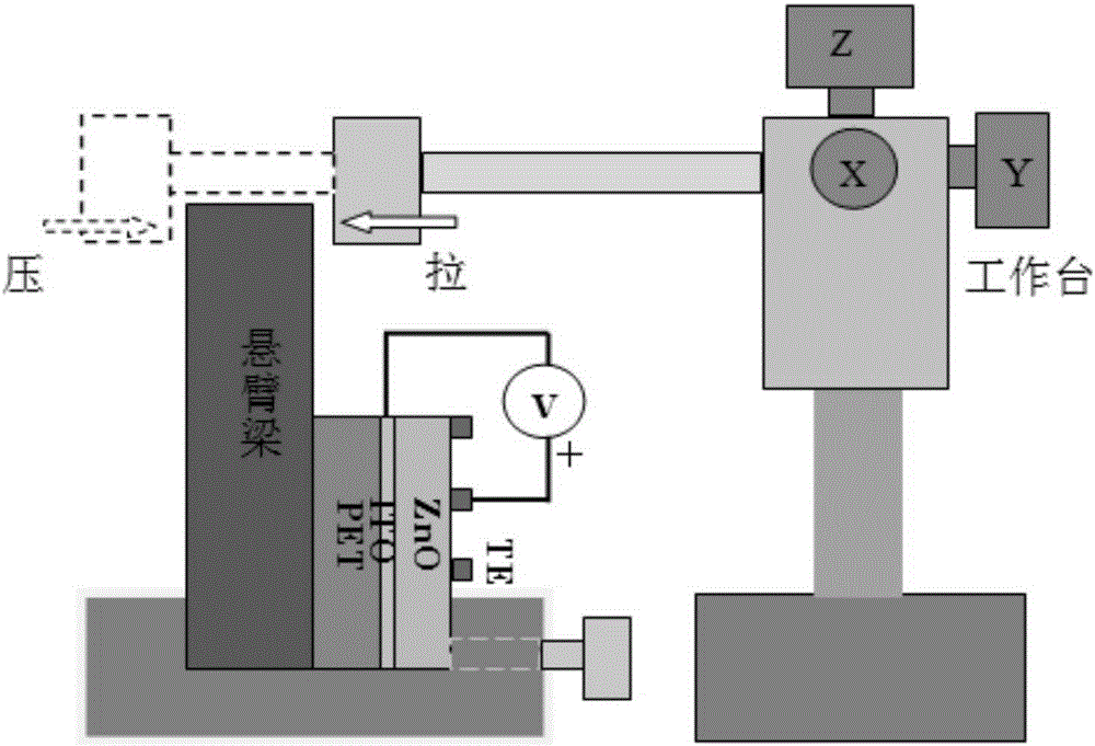
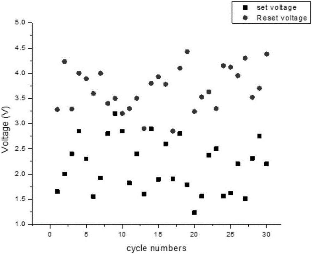
[0030] 3. Electrical performance test

[0031] By controlling the force act...

Embodiment 2

[0033] 1. RF magnetron sputtering of ZnO thin film

[0034] The ITO / PET substrates were super-cleaned in acetone, ethanol and deionized water respectively, and then dried with nitrogen. During the sputtering process, the system pressure was kept at 0.1 Pa, the Ar flow rate was 30 sccm, the sputtering power was 55 W, the deposition time was 60 minutes, and the film thickness range was 100 nm.

[0035] 2. Electron Beam Evaporation of the Metal Top Electrode

[0036] On the prepared ZnO thin film, place a stainless steel mask plate punched with round holes to cover the lower electrode and part of the ZnO thin film, and then send the sample and the mask plate into an electron beam evaporation coating apparatus. When the background vacuum of the chamber is pumped to 6×10 -5 When Pa, open the evaporation barrier to deposit a metal copper upper electrode with a thickness of 100 nm on the ZnO film.

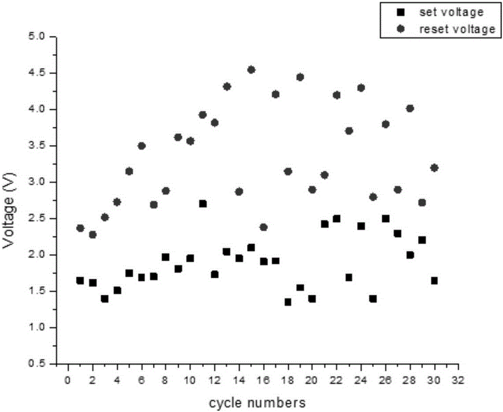
[0037] 3. Electrical performance test

[0038] By controlling the force acting on...

Embodiment 3

[0043] 1. RF magnetron sputtering of ZnO thin film

[0044] The ITO / PET substrates were super-cleaned in acetone, ethanol and deionized water respectively, and then dried with nitrogen. During the sputtering process, the system pressure was maintained at 0.3 Pa, the Ar flow rate was 20 sccm, the sputtering power was 55 W, the deposition time was 90 minutes, and the film thickness range was 150 nm.

[0045] 2. Electron Beam Evaporation of the Metal Top Electrode

[0046] On the prepared ZnO thin film, place a stainless steel mask plate punched with round holes to cover the lower electrode and part of the ZnO thin film, and then send the sample and the mask plate into an electron beam evaporation coating apparatus. When the background vacuum of the chamber is pumped to 6×10 -5 Pa, open the evaporation barrier to deposit a metal Au electrode with a thickness of 100 nm on the ZnO film.

[0047] 3. Electrical performance test

[0048] By controlling the force acting on the cant...


PUM


Abstract

The invention discloses a ZnO piezoelectric effect-based low-power consumption flexible resistance-variable memory and a preparation method thereof. The low-power consumption flexible resistance variable random-access memory (RAM) of the invention comprises a TE layer, a ZnO layer and an ITO / PET layer which are sequentially distributed from top to bottom, wherein the TE layer is made of Pt, Cu or Au of which the function is greater than a ZnO function. The method includes the following steps that: with an ITO / Pet flexible substrate adopted as a bottom electrode, a ZnO thin film is prepared through a sputtering method, and ZnO / ITO / PET can be obtained; and the ZnO / ITO / PET base body is arranged in a deposition chamber, and a metal upper electrode can be obtained through electron beam evaporation and by means of a mask method, so that a metal thin film electrode can be deposited on the ZnO thin film, and finally a flexible TE / ZnO / ITO / PET device can be obtained. According to the ZnO piezoelectric effect-based low-power consumption flexible resistance-variable memory and the preparation method thereof of the invention, set and reset voltage of the ZnO thin film layer can be adjusted and controlled through the piezoelectric effect of the ZnO thin film layer itself, and therefore, the operating voltage of the device can be decreased, and the power consumption of the device can be reduced, and the service life of the device can be prolonged.

Description

technical field [0001] The invention belongs to the technical field of nonvolatile resistive memory devices, and relates to a low power consumption nonvolatile flexible resistive random read memory. Background technique [0002] Random access memory (RAM) is an important form of computer data storage, mainly used as main memory (memory), with ultra-high access speed and write durability, such as the read and write time of static RAM (SRAM) Less than 0.3ns, read and write life can be as high as 10 16 Second-rate. However, RAM is volatile, and data is lost when power is turned off. Flash memory (flash memory) is currently the most advanced non-volatile memory, but it has a slow storage speed (10 5 ~10 6 ns), low endurance (write lifetime is about 10 5 times) etc. In addition, as the transistor tends to be sub-micron, a series of problems begin to appear, including the difficulty of manufacturing process and the limitation of device performance, such as the difficulty of ...

Claims


Application Information

Patent Timeline
Patent Type & Authority Applications(China)
IPC IPC(8): H01L27/24H01L45/00
Inventor 李红霞席俊华季振国
Owner 芜湖启博知识产权运营有限公司
Why Eureka
Try Eureka