Yttrium iron garnet film material and preparing method thereof

A technology of yttrium iron garnet and thin film, which is applied in metal material coating process, vacuum evaporation plating, coating, etc., can solve the problems of high cost, easy cracking of thin film, cumbersome process, etc., and achieve low dielectric loss and method The process is simple and easy, and the effect of low coercive force

Active Publication Date: 2016-02-17
SHANGHAI INST OF CERAMIC CHEM & TECH CHINESE ACAD OF SCI
View PDF5 Cites 10 Cited by
  • Summary
  • Abstract
  • Description
  • Claims
  • Application Information

AI Technical Summary

Problems solved by technology

Yttrium iron garnet thin films have been studied as circulators, isolators, memories and filters a lot. The phase shift devices of yttrium iron garnet thin films grown on Si substrates are compatible with the traditional Si planar CMOS process, but in Si Films grown on substrates are very prone to cracking and are

Method used


Image

  • Yttrium iron garnet film material and preparing method thereof
  • Yttrium iron garnet film material and preparing method thereof
  • Yttrium iron garnet film material and preparing method thereof

Examples


preparation example Construction

[0027] The present invention provides a kind of preparation method of the yttrium iron garnet thin film that sputtering epitaxy on Si substrate comprises the following steps:

[0028] Step 1: cleaning the substrate surface;

[0029] Step 2: sputtering a thin film on the substrate in a high vacuum environment;

[0030] Step 3: slow annealing of the film material.

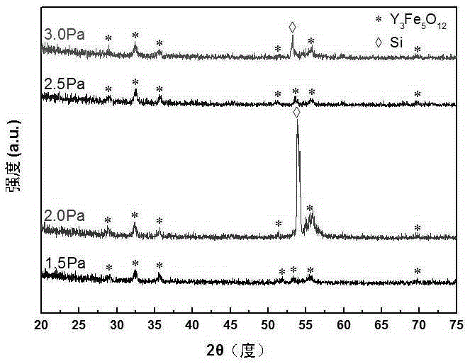
[0031] The substrate can be Si(100) / SiO 2 . Substrates can be purchased commercially or prepared by yourself. The substrate that adopts in the present invention is then purchased from commercial, and the substrate total thickness is about 0.5mm, and the SiO of one deck 300nm is covered on the surface 2 . Because the thermal expansion coefficients of Si and YIG are very different (Si is 4.7×10 -6 / °C, YIG is 10.4×10 -6 / ℃), adding a layer of SiO 2 (The coefficient of thermal expansion is 5.5×10 -6 / °C) can play a role in buffering thermal stress. Si substrates with different orientations can also be selected...

Embodiment

[0048] The present invention adopts figure 1 The shown equipment, sputtering yttrium iron garnet film, the specific preparation method is:

[0049] Step 1: First, clean Si(100) / SiO 2 The substrate surface, the cleaning process is:

[0050] (1) Ultrasonic cleaning with acetone for 10 minutes;

[0051] (2) Ultrasonic cleaning with alcohol for 10 minutes;

[0052] (3) Ultrasonic cleaning with deionized water for 10 minutes;

[0053] (4) drying.

[0054] Step 2: sputtering a thin film on the substrate in a high vacuum environment, the specific process is:

[0055] (1) Fix the cleaned substrate on the substrate table, Y 3 Fe 5 o 12 The target is fixed on the target table of the magnetron sputtering molding system, and both the substrate table and the target table are placed in the sputtering chamber of the magnetron sputtering molding system;

[0056] (2) Combining mechanical pump and molecular pump to evacuate the sputtering chamber until the indoor air pressure is lower ...


PUM

PropertyMeasurementUnit
Coercivityaaaaaaaaaa
Curie temperatureaaaaaaaaaa
Coercive fieldaaaaaaaaaa

Abstract

The invention relates to an yttrium iron garnet film material and a preparing method thereof. The preparing method includes the following steps that firstly, the surface of an Si/SiO2 substrate is cleaned; secondly, an yttrium iron garnet film is sputtered on the surface of the cleaned substrate through a radio frequency magnetron sputtering method, Y3Fe5O12 is adopted as the target material, background vacuum is smaller than 4.0*10-4 pa, sputtering gas is at least one of O2, N2 and Ar, sputtering pressure is 1.5-3.0 Pa, the temperature of the substrate ranges from room temperature to 600 DEG C, and sputtering power is 60-150 W; and thirdly, the yttrium iron garnet film prepared in the second step is subjected to post annealing. The film material prepared through the method has the beneficial effects that the structure is compact and is not cracked, saturation magnetization can be comparable to that of ceramic, the dielectric loss is low, coercive force is low, and the Curie temperature is far higher than the room temperature.

Description

technical field [0001] The invention belongs to the technical field of electronic materials, and in particular relates to a yttrium iron garnet film material sputtered epitaxy on a Si substrate and a preparation method thereof. Background technique [0002] Ferrite is a metal oxide with ferromagnetic properties. In terms of electrical properties, the resistivity of ferrite is much larger than that of metal and alloy magnetic materials, and it also has higher dielectric properties. Ferrite usually has a high magnetic permeability at high frequencies and low eddy current loss, and is suitable for making high-frequency electromagnetic devices. Therefore, it has become a non-metallic magnetic material with a wide range of applications in the field of high-frequency and weak currents. There are mainly three types of crystal structures of ferrite: spinel type, garnet type and magnetoplumbite type. According to different magnetic properties and uses, ferrite can be divided into f...

Claims


Application Information

Patent Timeline
IPC IPC(8): C23C14/35C23C14/08
CPCC23C14/083C23C14/085C23C14/35
Inventor 董显林连建芸陈莹王根水
Owner SHANGHAI INST OF CERAMIC CHEM & TECH CHINESE ACAD OF SCI
Why Eureka
Try Eureka