GaN-based field effect transistor with high quality MIS structure and preparation method of GaN-based field effect transistor

A MIS structure, high-quality technology, applied in semiconductor/solid-state device manufacturing, semiconductor devices, electrical components, etc., can solve problems such as degraded device stability, threshold voltage drift, etc., and achieve high process repeatability and reliability, high threshold Voltage stability, effect of improving mobility

Inactive Publication Date: 2016-02-17
SUN YAT SEN UNIV
View PDF3 Cites 14 Cited by
  • Summary
  • Abstract
  • Description
  • Claims
  • Application Information

AI Technical Summary

Problems solved by technology

Under different bias voltages on the gate, these interface states and defect charges will be charged and disc

Method used


Image

  • GaN-based field effect transistor with high quality MIS structure and preparation method of GaN-based field effect transistor
  • GaN-based field effect transistor with high quality MIS structure and preparation method of GaN-based field effect transistor
  • GaN-based field effect transistor with high quality MIS structure and preparation method of GaN-based field effect transistor

Examples


Example Embodiment

[0036] Example 1

[0037] Such as Picture 11 Shown is a schematic diagram of the device structure of this embodiment. The structure includes substrate 1, stress buffer layer 2, GaN epitaxial layer 3, secondary epitaxial layer 4, secondary epitaxial formation grooves, and tertiary epitaxial layer 5 from bottom to top. , The surface of the tertiary epitaxial layer 5 is oxidized to form an insulating oxide dielectric layer 6 with a source 7 and a drain 8 formed at both ends, and a gate 9 is covered on the insulating layer 6 at the groove channel.

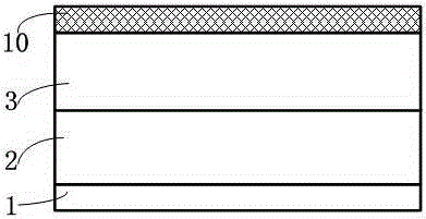
[0038] The manufacturing method of the above-mentioned high-quality MIS structure GaN-based field effect transistor is as follows Figure 1-Figure 10 As shown, including the following steps:

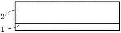
[0039] S1. Using metal organic chemical vapor deposition method to grow a layer of stress buffer layer (2) on Si substrate (1), such as figure 1 Shown

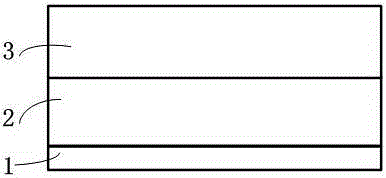
[0040] S2, using the metal organic chemical vapor deposition method to grow a GaN epitaxial layer (...

Example Embodiment

[0051] Example 2

[0052] Such as Picture 12 Shown is a schematic diagram of the device structure of this embodiment, which differs from the structure of Embodiment 1 only in that: the GaN / AlGaN heterostructure in Embodiment 1 is formed by secondary epitaxy and the gate groove region is naturally formed at the same time, while Embodiment 2 The medium GaN / AlGaN heterostructure is formed by one-time epitaxial formation and the gate groove area is formed by dry (or wet) etching. The reference number 11 is the primary epitaxial GaN / AlGaN heterostructure layer.

Example Embodiment

[0053] Example 3

[0054] Such as Figure 13 Shown is a schematic diagram of the device structure of this embodiment, which is different from the structure of Embodiment 1 only in that: Embodiment 1 is a lateral conduction device structure, and Embodiment 2 is a vertical conduction device structure. The substrate 12 is a heavily doped GaN free-standing substrate or a low-resistance silicon substrate or a low-resistance silicon carbide substrate, etc., 13 is a buffer layer, 14 is a lightly doped GaN drift layer, and 15 is a p-type doped GaN layer Or AlGaN layer. The vertical structure improves the chip power per unit area and effectively increases the breakdown voltage of the device.

[0055] In addition, it should be noted that the drawings of the above embodiments are only for illustrative purposes, and therefore it is not necessary to draw to scale.

[0056] Obviously, the above-mentioned embodiments of the present invention are merely examples to clearly illustrate the present i...


PUM

PropertyMeasurementUnit
Thicknessaaaaaaaaaa
Thicknessaaaaaaaaaa
Thicknessaaaaaaaaaa

Abstract

The invention belongs to the semiconductor material and device field and discloses a GaN-based field effect transistor with a high quality MIS structure and a preparation method of the GaN-based field effect transistor, in particular, a GaN MISFET device gate dielectric layer and an improvement method of a dielectric layer and GaN interface. The device includes a substrate, an epitaxial layer grown on the substrate as well as a gate electrode, a source electrode, a drain electrode and an insulating layer; the epitaxial layer includes a stress buffer layer which is formed through primary epitaxial growth, a GaN epitaxial layer as well as a second epitaxial layer and a third epitaxial layer which are grown on selective regions on the GaN epitaxial layer; a GaN/AlGaN heterostructure is formed through secondary epitaxial growth, and groove channels are formed; an AlN thin layer is formed through third epitaxial growth; the AlN thin layer is partially oxidized so as to form an AlN/oxide dielectric layer stack structure; gate metal covers the groove channels; a source electrode region and a drain electrode region are formed at two ends; and the source electrode region and the drain electrode region are covered with metal, so that the source electrode and the drain electrode can be formed. The device and preparation process of the invention are simple and reliable. With the preparation method adopted, the high quality MIS structure can be formed, and the performance of the GaN MISFET device can be improved. The preparation method can play a key role in decreasing the electric leakage of the gate electrode, decreasing the resistance of the channels and stabilizing threshold voltage.

Description

Technical field [0001] The invention relates to the technical field of semiconductor device preparation, and discloses a high-quality GaNMISFET structure and a preparation method thereof, in particular to a gate dielectric layer of a GaNMISFET device and a method for improving the interface with GaN. Background technique [0002] GaN semiconductor materials have the advantages of large forbidden band width, high breakdown electric field, high saturated electron drift speed and high thermal conductivity. GaN-based power switching devices usually use high-concentration and high-mobility two-dimensional electron gas at the AlGaN / GaN heterostructure interface to work, so that the device has the advantages of small on-resistance and fast switching speed, and becomes ideal for the next generation of power switching devices. alternatives. [0003] The realization of high-performance normally-off switching devices is an important challenge faced by GaN power electronic devices, and is cur...

Claims


Application Information

Patent Timeline
IPC IPC(8): H01L29/78H01L21/336
CPCH01L29/7801H01L29/66477
Inventor 刘扬何亮杨帆
Owner SUN YAT SEN UNIV
Why Eureka
Try Eureka