SOI pressure-sensitive chip based on sacrificial layer technology, and manufacturing method thereof

A technology of sensitive chips and sacrificial layers, which is applied in the direction of microstructure technology, manufacturing microstructure devices, and techniques for producing decorative surface effects, etc. It can solve the problems of poor performance such as sensor repeatability and hysteresis, and achieve repeatability and stability. Good performance, high sensitivity, good protection effect

Active Publication Date: 2016-03-30
SHENYANG POLYTECHNIC UNIV
View PDF6 Cites 8 Cited by
  • Summary
  • Abstract
  • Description
  • Claims
  • Application Information

AI Technical Summary

Problems solved by technology

However, due to the use of polysilicon strain resistance, the performance of the sensor such as repeatability and hysteresis is poor

Method used


Image

  • SOI pressure-sensitive chip based on sacrificial layer technology, and manufacturing method thereof
  • SOI pressure-sensitive chip based on sacrificial layer technology, and manufacturing method thereof
  • SOI pressure-sensitive chip based on sacrificial layer technology, and manufacturing method thereof

Examples


Embodiment Construction

[0043] The present invention will be further described below by accompanying drawing:

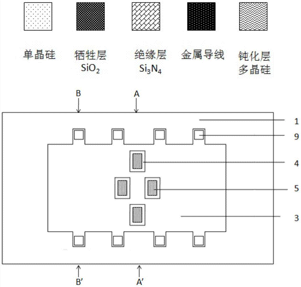
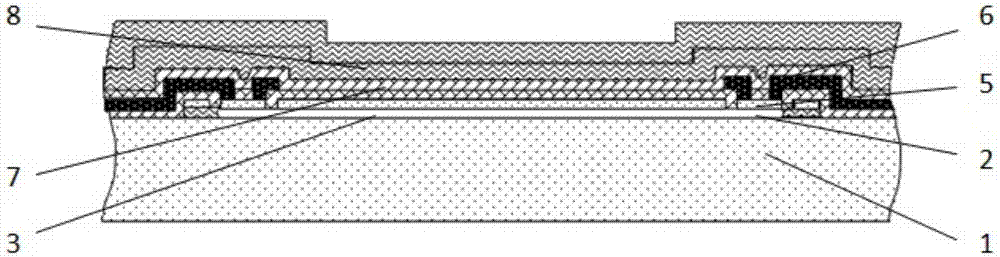
[0044] The invention provides a SOI pressure-sensitive chip based on sacrificial layer technology, such as figure 1 and figure 2 As shown, it is characterized in that: the chip is made of a single crystal silicon film (SOI) material on an insulating layer, including a single crystal silicon substrate 1 of SOI, and an SOI silicon dioxide insulating layer is used as a sacrificial layer above the single crystal silicon substrate 1 The cavity 2 is formed by layers, the top of the cavity 2 is a single crystal silicon film 3, and the isolation groove 4 is etched on the single crystal silicon film 3 to form four strain resistors 5 and their metal wires 6. The silicon nitride insulating protection layer 7 located above and below the metal wire 6 and the outermost polysilicon structure layer 8 and the single crystal silicon film 3 together form a sensitive chip pressure-sensitive film, and eight s...


PUM


Abstract

The invention discloses an SOI pressure-sensitive chip based on a sacrificial layer technology, and a manufacturing method thereof. The chip is manufactured by use of a monocrystalline silicon thin film (SOI) material on an insulation layer and comprises a monocrystalline silicon substrate of SOI, a cavity formed by taking an SOI silicon dioxide insulation layer as a sacrificial layer, four strain resistors formed by etching isolation grooves in the monocrystalline silicon thin film, and a metal lead wire. The silicon nitride insulation protective layer on and under the metal lead wire, an outermost polysilicon structure layer and the monocrystalline silicon thin film form a sensitive chip pressure-sensing film, and eight square holes are etched at the edge of the pressure-sensing film for corroding the silicon dioxide sacrificial layer. The four strain resistors are connected to form a Wheatstone bridge through the metal lead wire for converting pressure signals into voltage signals for output. The prepared SOI pressure-sensitive chip based on the sacrificial layer technology has the advantages of high sensing sensitivity, good repeatability and stability, high reliability, high-temperature resistance, radioresistance, compatibility between a manufacturing technology and an integrated circuit technology, and the like.

Description

technical field [0001] The invention mainly relates to an SOI pressure-sensitive chip based on sacrificial layer technology and a manufacturing method thereof. It belongs to the field of microelectromechanical systems (MEMS). Background technique [0002] Under the background that information technology continues to promote the rapid development of modern industry, MEMS sensors have attracted much attention, especially MEMS pressure sensors have been widely used in industrial production, aerospace, power petrochemical and other industries. At present, the diffused silicon pressure sensor is still the pressure sensor with the largest sales volume in the market, but the working temperature range of this piezoresistive sensor generally does not exceed 120°C, because the strain resistance of the diffused silicon pressure sensor uses the pn junction as the isolation layer to realize its electrically insulated from the substrate. However, when the operating temperature exceeds 1...

Claims


Application Information

Patent Timeline
Patent Type & Authority Applications(China)
IPC IPC(8): G01L1/22B81B3/00B81C1/00
CPCB81B3/00B81C1/00015G01L1/22
Inventor 揣荣岩衣畅张晓民关若飞关艳霞李新刘一婷
Owner SHENYANG POLYTECHNIC UNIV
Why Eureka
Try Eureka