Method for manufacturing three-dimensional capacitively coupled interconnection structure based on through-silicon capacitor

A capacitive coupling and interconnection structure technology, applied in the field of microelectronics, can solve the problems of reduced performance and yield, large occupied area, complex manufacturing process, etc., to reduce process equipment, reduce the impact of device performance and yield, and process shortening effect

Active Publication Date: 2016-04-06
XI AN JIAOTONG UNIV
View PDF10 Cites 10 Cited by
  • Summary
  • Abstract
  • Description
  • Claims
  • Application Information

AI Technical Summary

Problems solved by technology

[0003] The purpose of the present invention is to provide a method for manufacturing a three-dimensional capacitively coupled interconnection structure based on through-silicon capacitors, so as to solve the problem of lower performance and yield after three-dimensional integration of devices caused by the complex manufacturing process of TSV vertical interconnection structures, and the problem of

Method used


Image

  • Method for manufacturing three-dimensional capacitively coupled interconnection structure based on through-silicon capacitor
  • Method for manufacturing three-dimensional capacitively coupled interconnection structure based on through-silicon capacitor
  • Method for manufacturing three-dimensional capacitively coupled interconnection structure based on through-silicon capacitor

Examples


Embodiment 1

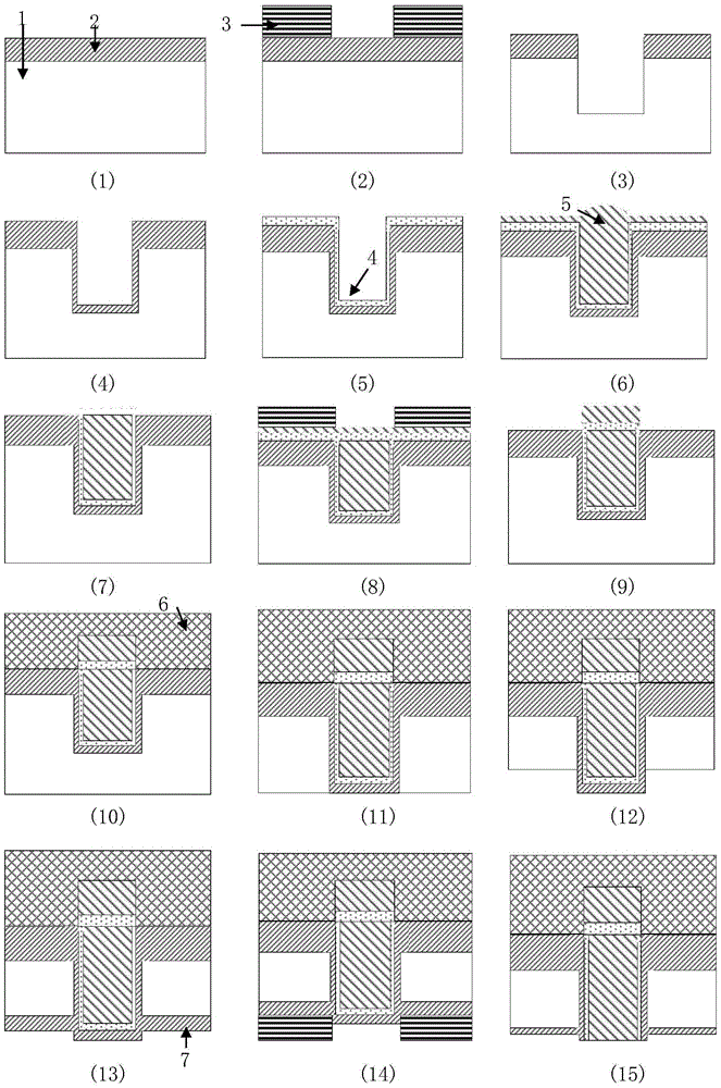
[0046] A method for manufacturing a three-dimensional capacitively coupled interconnection structure based on a through-silicon capacitor of the present invention, the wafer substrate used is P-type silicon, and the thickness of the silicon substrate is 675 μm, specifically comprising the following steps:

[0047] (1) growing a silicon dioxide mask layer 2 on the surface of the silicon substrate 1, the thickness of the mask layer is 2 μm;

[0048] (2) Coating photoresist on the surface of silicon dioxide mask layer 2 Expose and develop to expose the window W1 that needs to be etched on the top layer of silicon. This window is circular with a diameter of 5 μm;

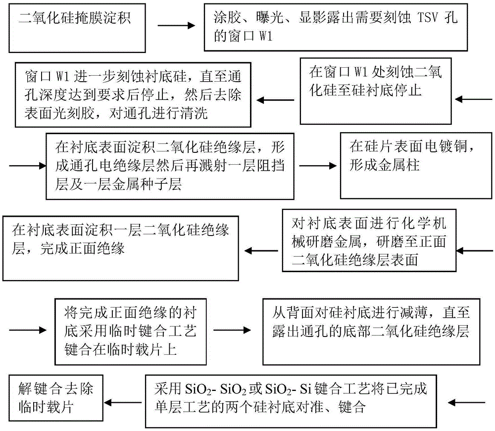
[0049] (3) Etch the silicon dioxide mask layer 2 at the window W1 until the silicon substrate 1 stops, and the etching depth is 2 μm; further etch the silicon substrate 1 at the window W1, and stop forming when the etching depth is 30 μm Through holes, then remove the surface photoresist 3, and clean the through holes...

Embodiment 2

[0061] A manufacturing method of a three-dimensional capacitively coupled interconnection structure based on through-silicon capacitors in the present invention adopts the SOI wafer substrate as P-type silicon, and the thickness of the buried oxide layer is Top Silicon Thickness Specifically include the following steps:

[0062] (1) Coating photoresist on the surface of SOI substrate Expose and develop to expose the window W1 that needs to be etched on the top layer of silicon. This window is circular with a diameter of 5 μm;

[0063] (2) Etch the top layer of silicon at the window W1 until the silicon dioxide buried oxide layer stops forming a through hole, and the etching depth is Then remove the surface photoresist and clean the through holes (deionized water + IPA + EKC);

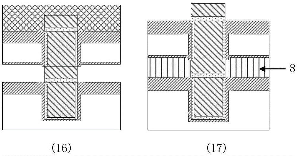
[0064] (3) Use PECVD (Ion Enhanced Chemical Vapor Deposition) method to deposit a layer of silicon dioxide insulating layer with a thickness of 1 μm on the surface of the substrate, so that the t...


PUM

PropertyMeasurementUnit
Thicknessaaaaaaaaaa
Depthaaaaaaaaaa
Thicknessaaaaaaaaaa

Abstract

The invention discloses a method for manufacturing a three-dimensional capacitively coupled interconnection structure based on a through-silicon capacitor. The method comprises: forming two silicon substrates same in structure by machining, and bonding the back surface of one silicon substrate to the other silicon substrate in an alignment manner; forming the three-dimensional capacitively coupled interconnection structure based on the through-silicon capacitor; coaxially arranging copper columns at the upper part and the lower part of the interconnection structure; enabling the top of the copper column at the lower part to be in contact with a silicon dioxide insulation layer on the back surface of the silicon substrate at the upper part; and taking the copper column at the upper part and the copper column at the lower part as an upper electrode plate and a lower electrode plate of the capacitance respectively, taking an insulation layer between the copper column at the upper part and the copper column at the lower part as an inter-capacitance medium, and forming a through-silicon capacitor structure. Compared with a conventional TSV process, the method has the characteristics that the technological processes of making metal convex points on the front surface of a wafer, thinning the back surface to expose copper, performing insulation treatment, making micro-convex points and the like in a TSV structure making process are removed, the technological processes are remarkably reduced, the yield is increased, and required process devices are correspondingly reduced.

Description

technical field [0001] The invention belongs to the technical field of microelectronics, and in particular relates to a manufacturing method of a three-dimensional capacitive coupling interconnection structure. Background technique [0002] Currently commonly used three-dimensional integrated interconnection structures mainly include through-silicon vias (TSV: Through Silicon Via) and capacitive / inductive coupling. TSV originated from the US patent "Semiconductive wafer and method of making the same" (3,0044,909) filed by William Shockley in 1958, which used the "deeppits" structure to realize signal transmission from the front to the back. The TSV vertical interconnection structure is based on the structure proposed in the literature "Through Silicon Via Technology–Processes and Reliability for Wafer-Level 3D System Integration" (Ramm, P. and Wolf, M.J published in ECTC58th in 2008) and "Through-Silicon Via (TSV)" (MakotoMotoyoshi published in Proceeding of the IEEE in 2009...

Claims


Application Information

Patent Timeline
IPC IPC(8): H01L23/48H01L21/768
CPCH01L21/768H01L23/481
Inventor 单光宝刘松耿莉
Owner XI AN JIAOTONG UNIV
Why Eureka
Try Eureka