Highly conductive substrate and manufacturing method thereof

A high-conductivity, manufacturing method technology, applied in cable/conductor manufacturing, conductive layers on insulating carriers, circuits, etc., can solve problems such as high equipment requirements, poor light transmittance of thin films, and inability to synthesize graphene. The effect of low impurity content, good electrical conductivity and light transmission

Inactive Publication Date: 2017-09-01
GOLD CARBON CO LTD
View PDF5 Cites 0 Cited by
  • Summary
  • Abstract
  • Description
  • Claims
  • Application Information

AI Technical Summary

Problems solved by technology

Among them, although graphene with better quality can be obtained by mechanical exfoliation and epitaxial growth, neither of these two methods can synthesize large-area graphene.
In addition, although high-quality graphene with a relatively perfect structure can be obtained by chemical vapor deposition, this method must use a production process temperature of nearly 1,000 degrees and expensive metal substrates (such as copper or nickel), so there are still requirements for equipment. higher defect
[0010] The chemical exfoliation method can be roughly divided into two methods: ultrasonic vibration (ultrasonication) exfoliation or ion intercalation of graphite materials, and exfoliation of oxides from graphite oxide blocks. Although the chemical exfoliation method has the advantages of large-scale mass production and solution solution processed fabrication and easy subsequent chemical functionalization, etc., but it may lead to the problem of poor light transmittance of the film

Method used


Image

  • Highly conductive substrate and manufacturing method thereof
  • Highly conductive substrate and manufacturing method thereof
  • Highly conductive substrate and manufacturing method thereof

Examples


no. 1 example

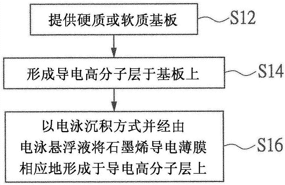
[0041] Please refer to figure 1 , is a schematic flow chart of the manufacturing method of the highly conductive substrate according to the first embodiment of the present invention. Please cooperate with reference Figures 2A to 4B , for the corresponding figure 1 Schematic diagram of the fabrication process for each fabrication process step. first as figure 1 As shown, the manufacturing method of the highly conductive substrate of this embodiment mainly includes: step S12, providing a hard or soft substrate; step S14, forming a conductive polymer layer on the substrate; and step S16, electrophoretic deposition and via The electrophoretic suspension forms the graphene conductive film on the conductive polymer layer accordingly.

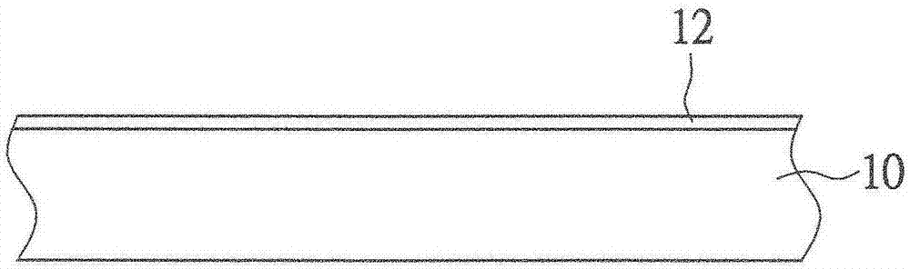
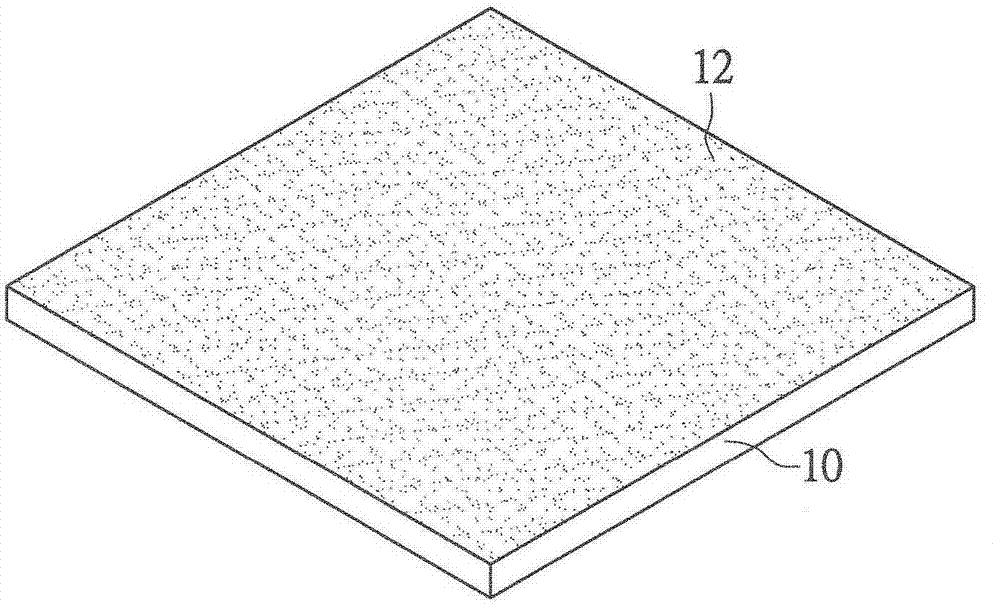
[0042] Please cooperate with reference Figure 2A and 2B , the manufacturing method of this embodiment first provides a hard or soft substrate 10 (step S12). In practical implementation, the hard substrate may be a metal substrate, a quartz su...

no. 2 example

[0050] Please refer to Figure 5 , is a schematic flow chart of the manufacturing method of the highly conductive substrate according to the second embodiment of the present invention. Please cooperate with reference Figures 6A to 7B , for the corresponding Figure 5 Schematic diagram of the fabrication process for each fabrication process step. first as Figure 5 As shown, the manufacturing method of the highly conductive substrate of this embodiment mainly includes: step S22, providing a hard or soft substrate; step S24, forming a conductive polymer layer on the substrate; step S26, patterning the conductive polymer layer; And step S28 , correspondingly forming the graphene conductive film on the patterned conductive polymer layer by means of electrophoretic deposition and via the electrophoretic suspension.

[0051] Please cooperate with reference Figures 6A to 7B The manufacturing method of this embodiment firstly provides a hard or soft substrate 10 (step S22 ). Si...


PUM

PropertyMeasurementUnit
electrical resistivityaaaaaaaaaa
transmittivityaaaaaaaaaa

Abstract

The present disclosure relates to highly conductive substrates and methods of making the same. A method for manufacturing a high-conductivity substrate, comprising the following steps: firstly, a substrate is provided; then, a conductive polymer layer is formed on the substrate; finally, a graphene is conductively deposited by electrophoretic deposition through an electrophoretic suspension A thin film is correspondingly formed on the conductive polymer layer, wherein the electrophoretic suspension contains 250 to 750 ppm of graphene dispersion and electrolyte. Compared with the existing production process in the industry, the new method disclosed by the invention is easy to control, easy to operate and low in cost, and has considerable economic value and wide applicability. The present invention further discloses a high-conductivity substrate manufactured by the above-mentioned manufacturing method.

Description

technical field [0001] The invention relates to a manufacturing process of a conductive thin film, in particular to a manufacturing method of a high-conductivity substrate using electrophoretic deposition technology. Background technique [0002] For a long time, people have been committed to the research and development of various optoelectronic components such as liquid crystal displays, solar cells, and light-emitting diodes. Compared with other conductive materials, indium tin oxide (ITO) is distinguished by its high conductivity and light transmittance. Become the main transparent conductive film material today. However, ITO has problems such as high production costs and rising prices due to the scarcity of raw materials. At the same time, the brittleness of ITO makes it unable to meet the performance requirements of some new applications. Therefore, the industry has tried to develop alternative materials for ITO. [0003] Graphene has many excellent properties, which ...

Claims


Application Information

Patent Timeline
Patent Type & Authority Patents(China)
IPC IPC(8): H01B13/00H01B5/14
Inventor 谢建德陈钰夫林友复魏荣宗
Owner GOLD CARBON CO LTD
Why Eureka
Try Eureka